
PCB Design
To verify our HR/RR rate monitoring system, we designed a 2-layer PCB to cooperate our chip with the off-chip components, our PCB design software was using KiCad. The PCB design consisted of our off-chip low/high pass filter of different OTA stage, Low Dropout Linear Regulator, two voltage regulators for DC bias voltage and reference voltage for comparator, infrared light emitting diode as well as the photo transistor, Arduino UNO-3 Microcontroller, and an LCD screen. The voltage supply for different components was solved in the following: 5V for infrared LED and phototransistor was provided by the Arduino board, 1V chip supply voltage was provided by the LDO (input voltage is 5V), 0.5V for DC bias voltage and 0.575V for reference voltage of comparator provided by two separate voltage regulator.
Figure12 and Figure 13 respectively show the PCB schematic and Layout, for detailed PCB schematic and Layout, please refer to the following link.
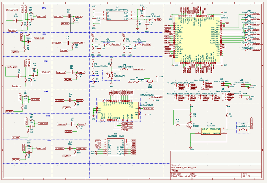
Fig. 12. PCB Design Schematic
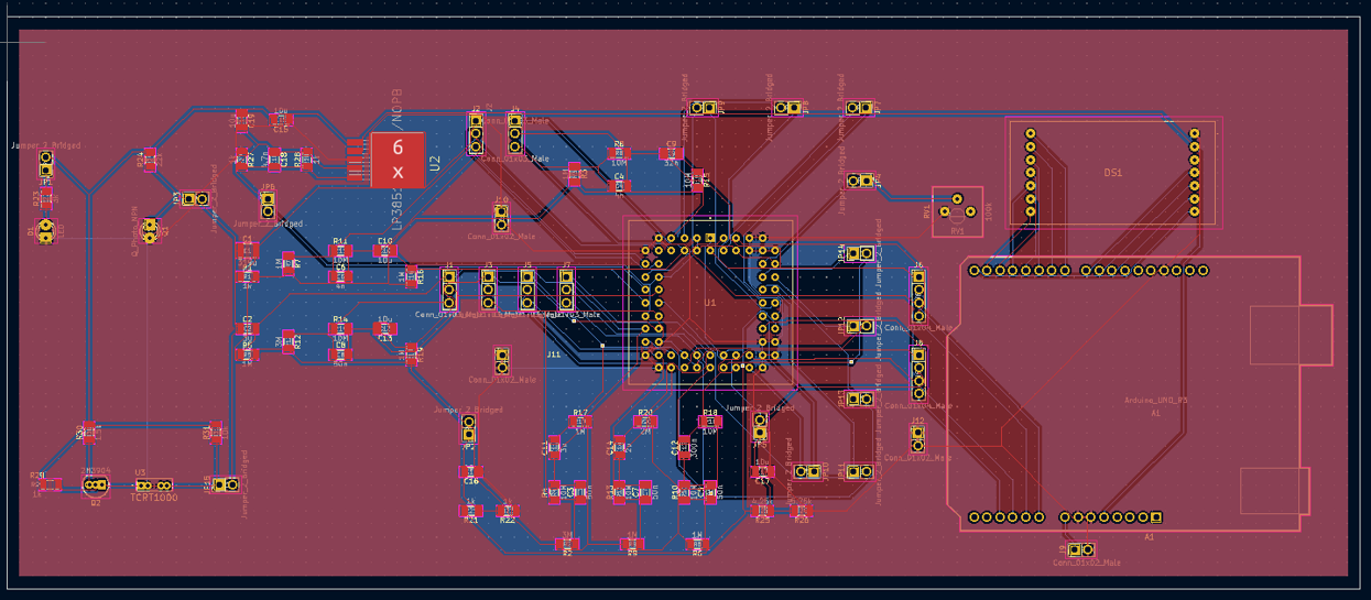
Fig. 13. PCB Design Layout
Arduino Board Source Code
For our system, we use Arduino board to process comparator output signal, the output signal of Heart rate and Respiratory rate will be processed and calculated on Arduino and displayed on the LCD screen.
To reduce the measurement errors, we take the average method for the continuous signal measurement. For both heart rate and respiratory rate signal, we will neglect the first three pulse because of the imprecise measurement of the fluctuation of infrared LED and phototransistor. Note that the system can also show the instantaneous heart rate and respiratory rate.
The Arduino source code can be Download at here .