System Overview
Introduction and Background
The use of image sensors presents several limitations for visible light spectrometers. Both CCD and CMOS one dimensional imagers typically use a global shutter, which is activated for a fixed time period determined by the control electronics. After the image is captured, each individual photodetector element is serially read out of the system through a multiplexer and shared charge amplifier. This process is time-consuming, and also relies on an estimate of the incoming signal to set the amplifier gain and integration time to avoid saturation of the brightest pixel. This effect also limits the dynamic range of the system. The nominal dynamic range is quite large – for the TAOS/ams 1401, for example, more than 1000:1 range can be achieved within a single exposure, and the exposure duration can be modulated over a further 3000:1 range. If the exposure time is incorrectly estimated or the difference between the bright and dark pixels is large, however, the net dynamic range is compromised and the full range is not realized. Overexposure/saturation can also lead to blooming and contribute noise to neighboring pixels.
In this project, we design an image sensor integrated circuit that offers the potential for high dynamic range operation by digitizing light output at the pixel level. The design was carried out using the 180nm, IBM 7RF technology development kit. In what follows is a brief account of the design process , and some simulation and measured results.
Concept overview:
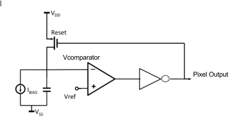
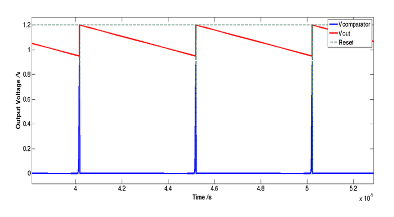
The basic schematic of one pixel of the proposed imager is shown below. Incident light is sensed using a reverse biased CMOS photodiode. The photodiode can be modeled as a current source representing charge generation from incident light and a parasitic capacitor, corresponding to the diode junction capacitance, in parallel with the current source. The capacitor is initially charged to the supply voltage Vdd and the reset transistor is open circuited. Incident light causes the capacitor to discharge and subsequently the capacitor voltage decreases. As soon as the capacitor voltage crosses a threshold Vref, the comparator block switches low. The switching output of the comparator passes through an inverting buffer and turns on the reset switch. The reset switch charges the capacitor back to Vdd. As the capacitor voltage increases, the comparator switches high. Once again the switching output of the comparator propagates through the inverting buffer, and after some delay depending on the buffer capacitance, the reset switch is open circuited once again. Subsequent illumination of the diode repeats the above cycle. At the output node,Pixel Output, a pulse edge is observed. As a result of the above operation, the circuit converts a quantum of incident light into a pulse train. The intensity of the incident light is encoded in the frequency of the pulse train with larger frequency corresponding to higher illumination intensity and vice versa. The waveforms below demonstrate the operation of the pixel by highlighting the outputs of three nodes in the circuit during operation.