Layout
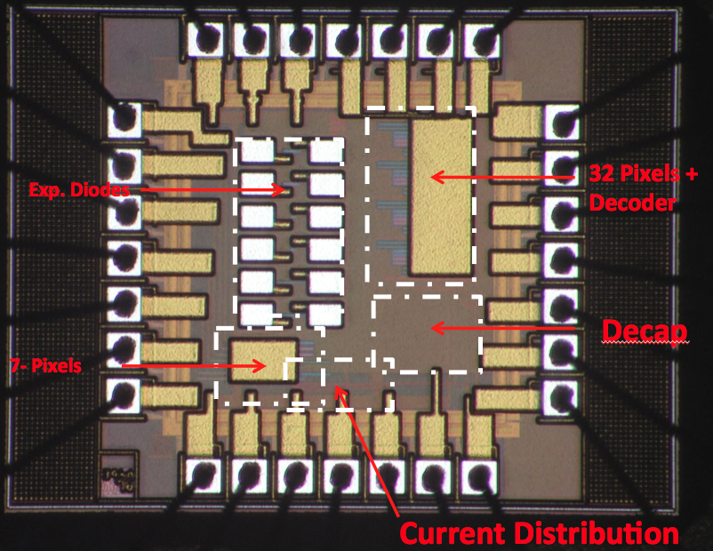
Die Photograph

IC Layout
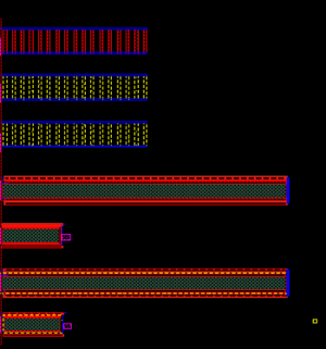
Shown below are the physical layouts of the chip and important consituent blocks in addition to the die photo of the fabricated chip.
OTA design incorporated cross-coupled feedback transistors to improve the slew rate using positive feedback. The design was simulated under varying process corners (TT,SS,SF,FS) and no degradation in the switching behavior was observed due to “latching” effects stemming from positive feedback. To address mismatch and subsequent DC offsets that can stem from that, care was taken to layout any nominally matched devices in the OTA in a symmetrical fashion. Furthermore, most devices are interdigitated to reduce the impact of process gradients across the die area. As shown below, each pair of devices that require matching (highlighted in blue) are fingered and interdigitated.

Pixel Layout
DiodeLayout
Shown below are the physical layouts of the chip and important consituent blocks in addition to the die photo of the fabricated chip.
A key element in the design of the photodiode pertained to its layout. The layout must introduce minimal parasitic resistance and capacitance.. A number of different photodiode geometries were implemented in the design. The design variations included different diode active area and different layer stacks for the diodes. It is well known that the spectral responsivity of a PN junction photodiode depends on the width of the diode depletion region with peak responsivity moving to shorter wavelengths (closer to blue light) for thin depletion widths and longer wavelengths (closer to red light) for large depletion widths. However, most integrated circuit fabrication processes do not offer the user any explicit control over vertical layer dimensions. One method for varying junction width of a vertical PN diode is to use different doping levels for the constituent P-type and N-type layers. Higher doping levels result in thinner depletion regions. In this design, we implemented both N+/P-substrate and N-well/P-substrate diodes (Fig.3). Due to the lower doping levels of the N-well, the N-well/P-substrate structure should exhibit a wider depletion region than the N+/P-substrate diode. Finally, a fingered geometry was also implemented. as shown below. The fingered geometry consists of multiple photodiodes placed in parallel. The fingering reduces the active area of the photodiode by some amount when compared to a non-fingered diode of the same perimeter. However, the fingered design has been demonstrated to improve charge collection efficiency (i.e. sensitivity) and reduce dark current noise. In total, six different diode types were implemented, namely N+/P-substrate and N-well/P-substrate non-fingered diodes in two sizes (10umx35um and 10umx100um) and fingered N+/P-substrate and N-well/P-substrate diodes in one size (100umx35um). Furthermore, the layout mask ensures metal-masking of all circuit elements except the photodiode active area to prevent undesired illumination-induced photocurrents during testing of the system. The photodiode layouts also include a special metal-fill exclusion to prevent automated metal-filling above the photodiode active areas which would block incoming light.