
Testing
Process Corner Characterization
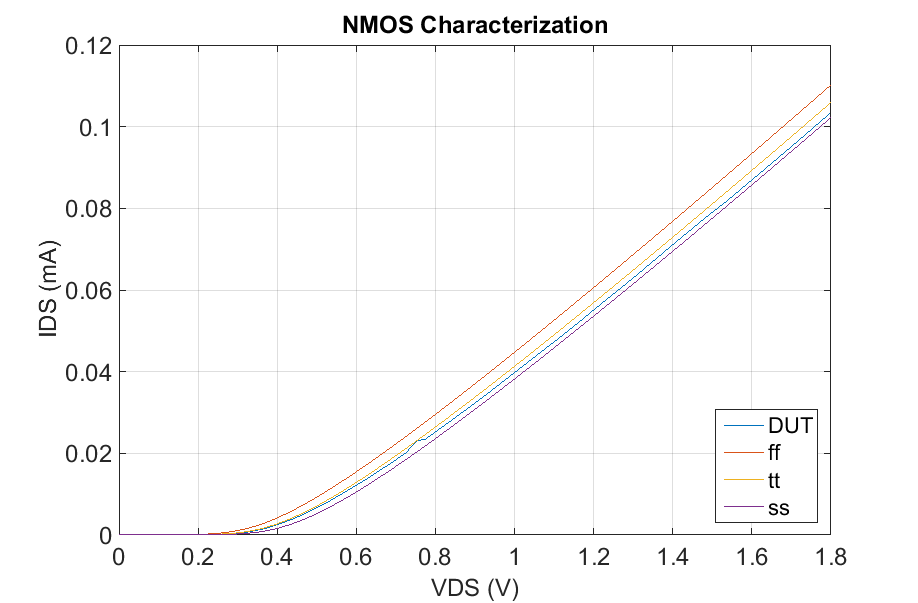
The process corner affects the performance of various circuit blocks and ultimately the IC. Although during the design process, extra caution was place to minimize its effect, it is still prudent to determine the process corner of the fabricate IC to help understand performance variation of the device under test.
Using the diode-connected 10um/1um NMOS on-chip, a DC voltage is applied to the test pin (26) to determine the IV characteristic. Compared to the simulated I-V curve of various process corners, it was determined the chip we have is between the tt and ss corner, as shown below.
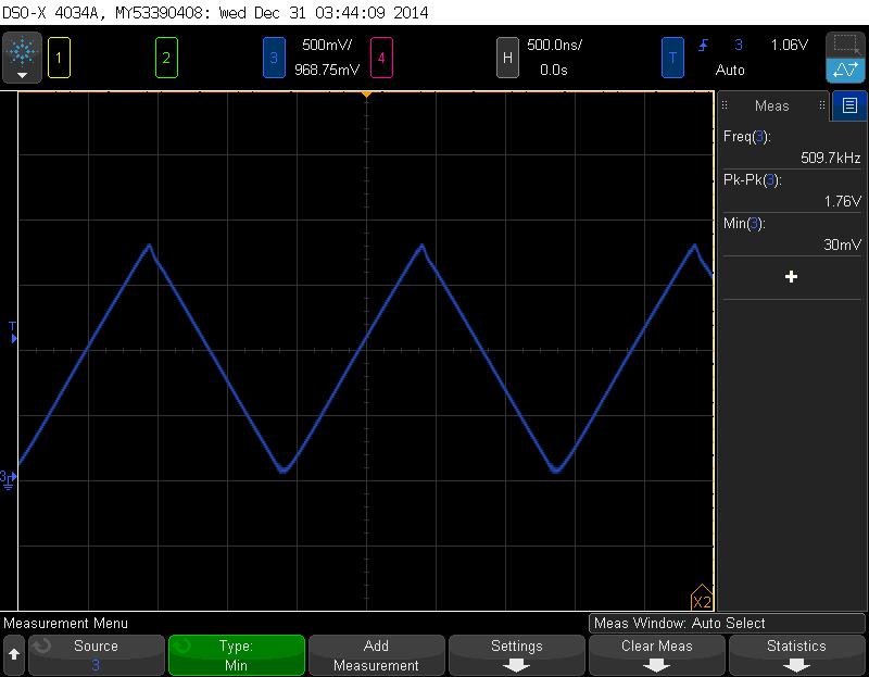
Triangular Wave Generator
The following screen capture verifies the functionality of the on-board triangular wave generator. The output frequency is at 509kHz, about 1.8% off designed 500kHz. The voltage swing is close to VDD at 1.76V.
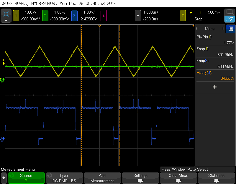
Pulse Width Modulation
To ensure that the IC functions as a pulse width modulator, a small DC offset voltage around VCM (0.9V) is applied to the input. The following screen capture shows the PWM waveform at the PWMP pins, with the output LPF and load resistor disconnected. The duty cycle is indeed proportional to the input magnitude.
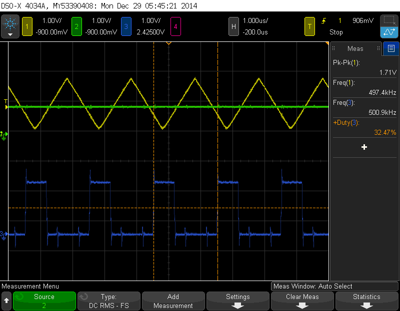
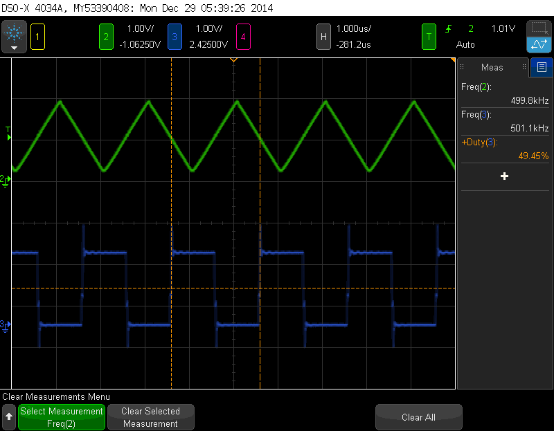
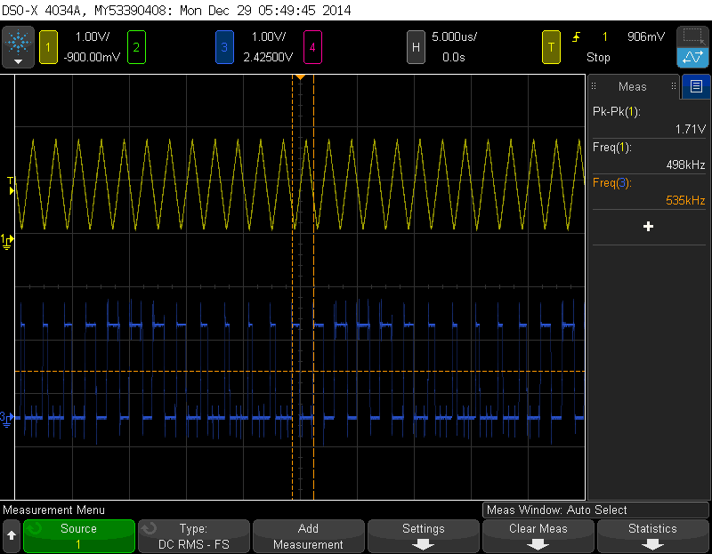
A 50kHz sine wave is subsequently applied to the input. As expected, the duty cycle varies depending on the instantaneous sine wave magnitude.
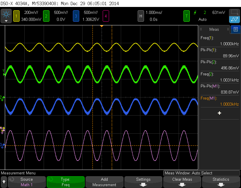
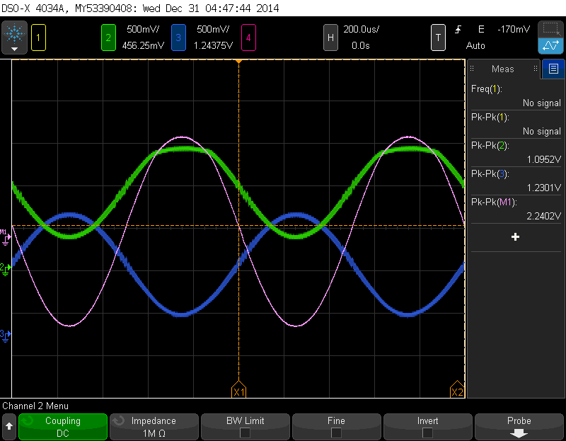
Input/output Characteristic
After the LPF and load resistor are connected, the following screen capture was made to observe the input and output waveform of a 1kHz sine wave input. The non-inverting output has a gain of 5.31 and the inverting output has a gain of 5.611. This variation (+6%/+12%) from designed gain of 5 can be attributed to the on-chip input resistor that determines the gain in the overall feedback loop, which can be up to 20%. It also conforms to the previously characterization that this chip is made in the ss corner. The overall differential gain (displayed using the oscilloscope's math function) is 9.31, or 19.38dB.
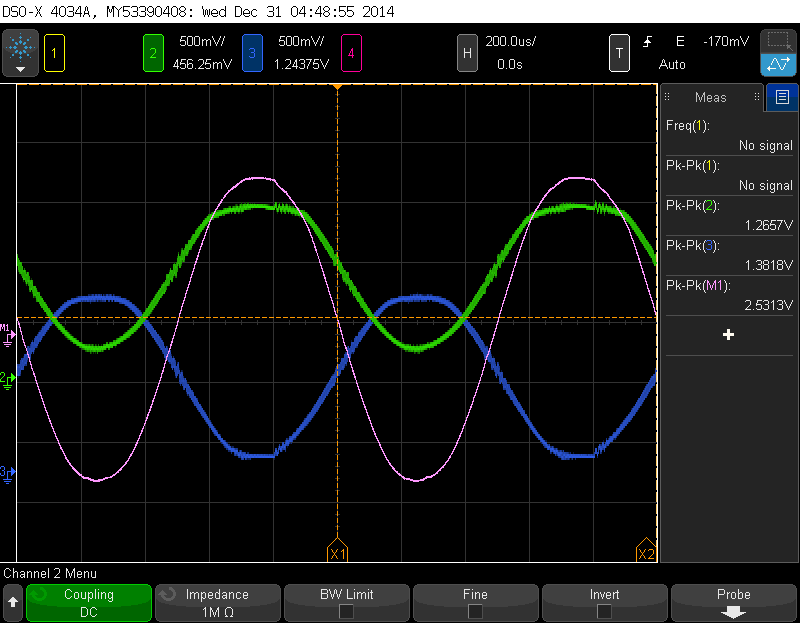
The 1kHz sine wave input magnitude is then swept to observe gain linearity, as shown below.
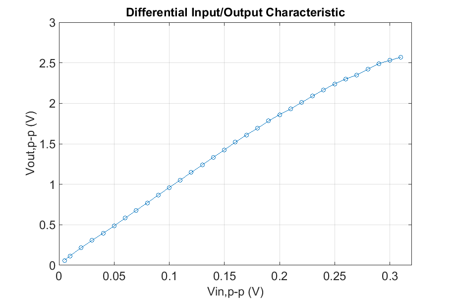
Clipping begins at 250mVp-p input, corresponding to a 2.25Vp-p output range. The following screen captures observed the clipping output response.
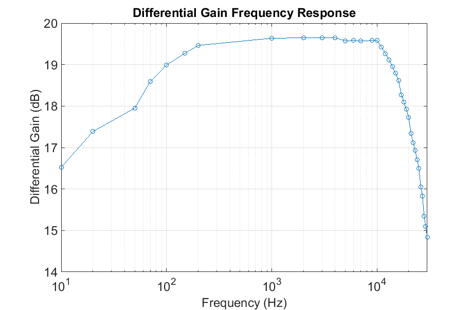
Frequency Response
The gain frequency response is largely dominated by the output LPF, which is designed for a 28kHz -3dB point. The low frequency roll off is a result of the capacitive AC coupling at the input, to both isolate the input source and provide the common mode DC offset. As expected, the -3dB bandwidth is between 10Hz to 25kHz, covering the entire audio band of 20Hz-22kHz.
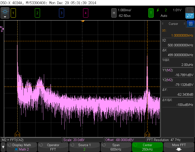
Frequency Spectrum Capture
The oscilloscope has a built in FFT function to allow frequency spectrum captures. To validate its use, the following capture shows the PWM spectrum taken for the differential output. It is evidential that the 500kHz modulating signal is still present, but over 80dB below the fundamental. These both verify the oscilloscope FFT function as well as the LPF performance of suppressing high frequency content of the PWM modulation. From here on, all spectrum plots are made by measuring frequency content in the units of VRMS and importing data into MATLAB for processing.
Distortion
In a Class-D design, the major source of distortion comes from the deadtime at the output stage driver. In addition, the gain variation between inverting and non-inverting output and output filter linearity will also affect the distortion. Distortion in audio amplifier is typically measured using Total Harmonic Distortion, or THD. It the ratio between the root mean square of the all harmonics to the fundamental tone, as expressed in,
Since this is an audio amplifier, all the harmonics that are summed will be within the 20Hz-22kHz band.
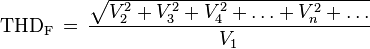
One of the benefits of using a differential output is the complete cancellation of even order harmonics, thus lowering the THD. However in actual design, gain variation and channel imbalance will cause imperfect cancellation. The following plots of the frequency spectra of the single-ended and differential output will allow us to access the improvement. They are both referenced to the fundamental tone at the output.
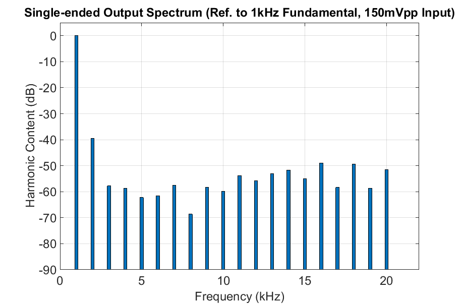
Comparing these spectra, it is evident that the even order harmonic cancellation works very well, pushing the second order harmonic down to -85dB. The single-ended output has a THD of 1.32% while the differential output THD is 0.23%, representing a more than five-fold improvement.
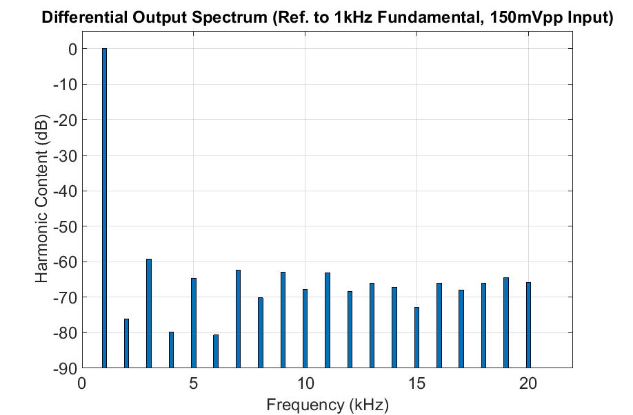
Figure 15 below demonstrate the effect of output power on THD. The lowest THD of 0.23% is observed at 150mVp-p input. At lower output power, noise and internal small signal linearity limits the THD, while at higher output power, the clipping characteristic quick raise the distortion. We can expect THD less than 1% between 30mW to 90mW.
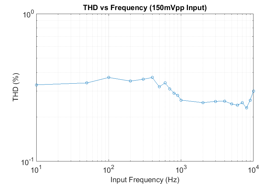
Figure 16 shows the variation of THD against frequency. After 1kHz, the THD drops significantly, because less harmonics are being summed, up to 22kHz. However, throughout the audio band, THD remained below 0.3%.
Efficiency
Class-D design inherently possesses higher power efficiency than linear class amplifier. In theory, it can deliver 100% of the power drawn from power source to the load, since the output devices are operating in either ON or OFF state, instead of saturation or active region in the linear amplifier. However, the PWM modulator, the integrator and the driver circuits within the CU6350, and the switching loss at the output devices and the will result in lower efficiency. In the following figure, the power efficiency is plotted against output signal power. This is after all additional current drawn for auxiliary circuits on the testing board are removed, thus observe only the efficiency of the IC.
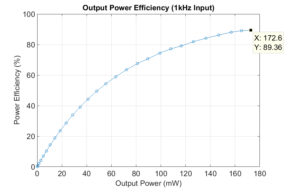
As expected, at lower output power, the power used for the single-ended to differential convert, integrator, comparator and driver dominates the current consumption, thus the low efficiency figure. As output power increase, the signal power dominates the current draw, and the efficiency rises to a maximum of 89%.