PCB Design
Evaluation board
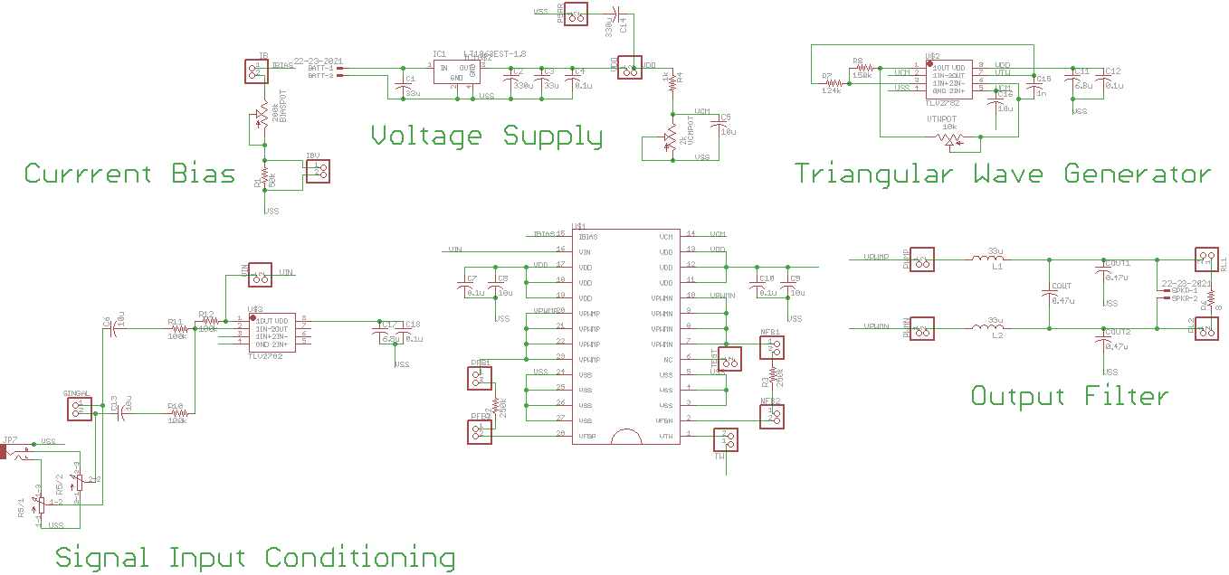
The overall layout of the chip consists mirrored blocks of the integrator, dead time generator and output stage, after the single-end-to-differential converter. It strives for symmetry because of the differential design. VDD and GND pins routes power from the corners of the chip, and outputs are on the top and bottom center pins. Signal inputs are routed via the left and right center pins to minimize power supply noise.
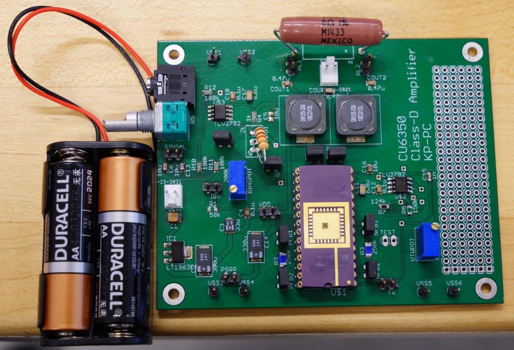
Most components are SMD, due to the small size of the board and consideration for the shortest trace possible. The board has two-layers and both are covered by a large ground plane. Special attention is taken to shorten the traces where PWM waveform travels, since they are most likely to couple to other circuits. A section of spare headers are reserved for any additional circuit needed during testing.
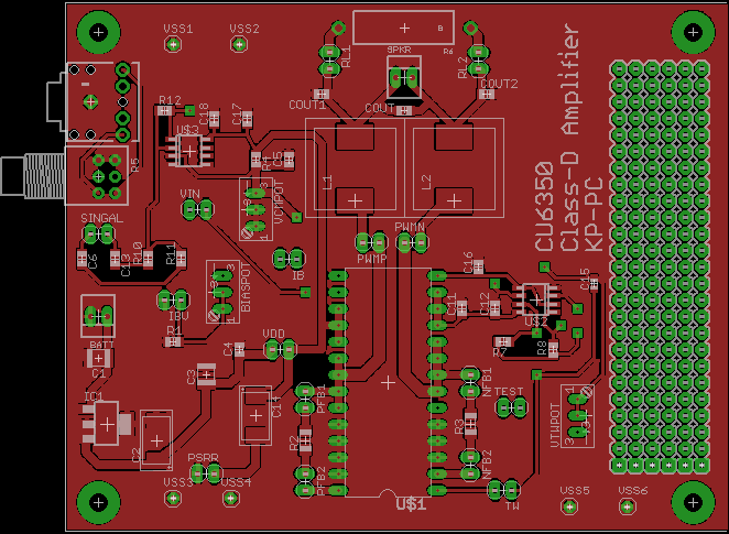
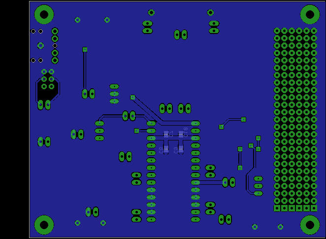
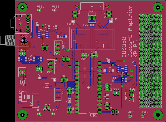
Figure 5 below shows the complete PCB, populated with all components.