
Component Design
1. OTA Design
We chose two stage differential topology as a reference to design our OTA. The reason we chose this topology is that two stage differential topology provides us enough voltage gain while still guarantee enough swing. We use NMOS as amplify transistor as NMOS has greater transconductance compared to PMOS at same working conditions. The detailed OTA parameter is shown in Fig. 4. 3. Fig. 4. 2 shows the testbench we use to test the loop gain of our OTA. We use a big inductor and a small capacitor to cut off the feedback loop and set feedback to zero when running AC simulation, this is to get the loop response of designed OTA. We add another OTA at the output of our test OTA to simulate the load of our OTA at working scenario.
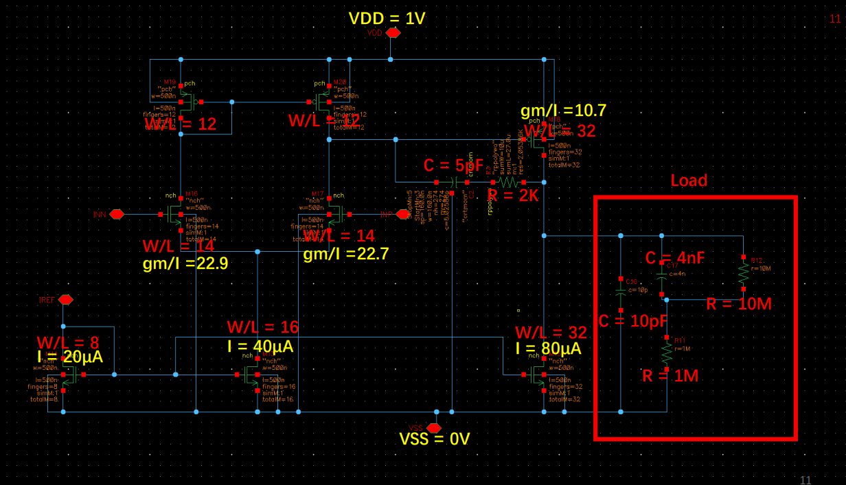
Fig. 4. 1. OTA Schematic
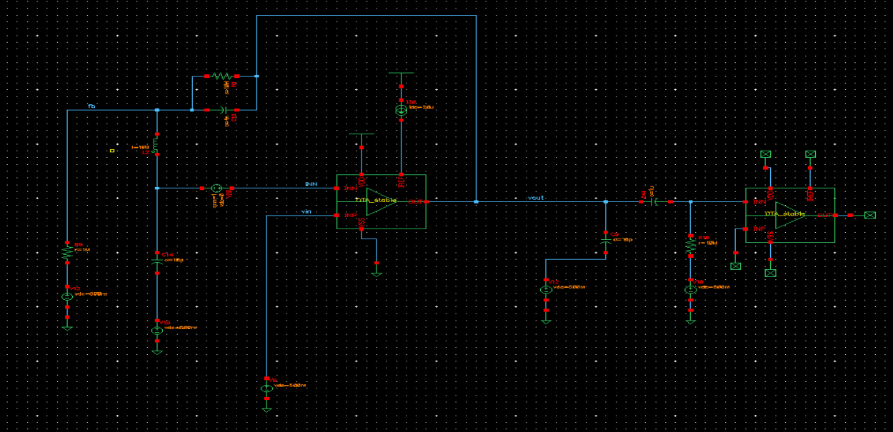
Fig. 4. 2. OTA Property Testbench
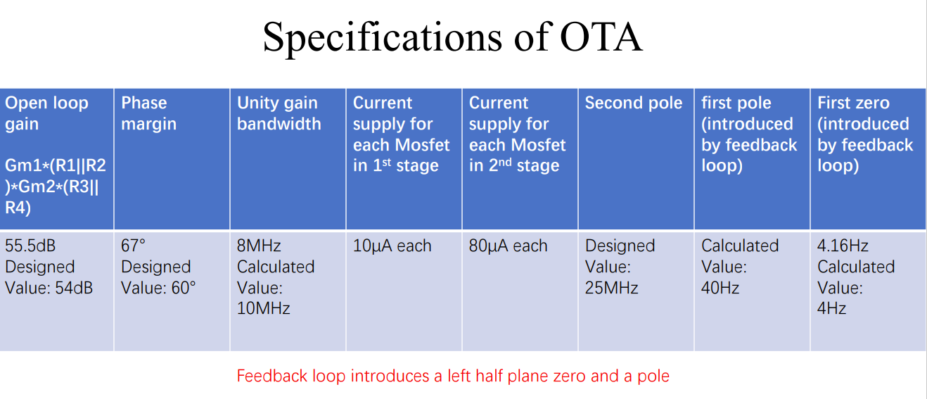
Fig. 4. 3. OTA Design Specification
Fig.5. shows the simulation result of the loop gain of designed OTA under different working conditions. It also shows the value of open loop gain with regards to each condition. Fig.6. shows the step response of designed OTA. Its step response proves the stability of designed OTA.
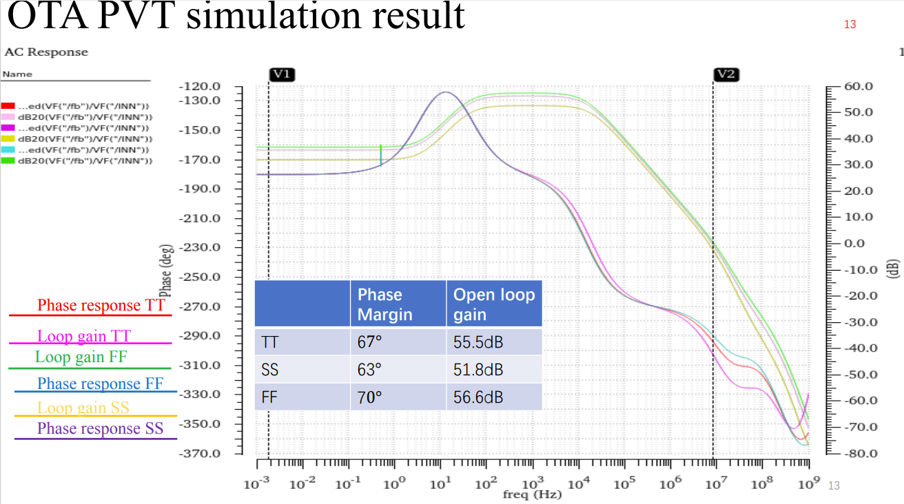
Fig. 5. OTA Simulation, Loop Gain
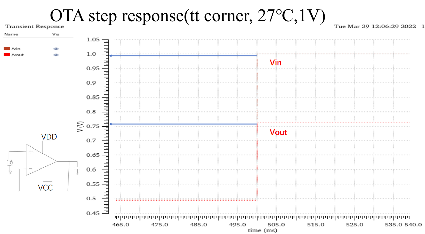
Fig. 6. OTA Step Response
2. Comparator Design
As for comparator, we use hysteresis comparator. As the output signal of our OTA still contains noise, using hysteresis will help us get cleaner signal and thus give us more accurate results for heart rate and respiratory rate frequencies. Fig. 7 shows the detailed design specification of comparator and its output voltages under different input voltages.
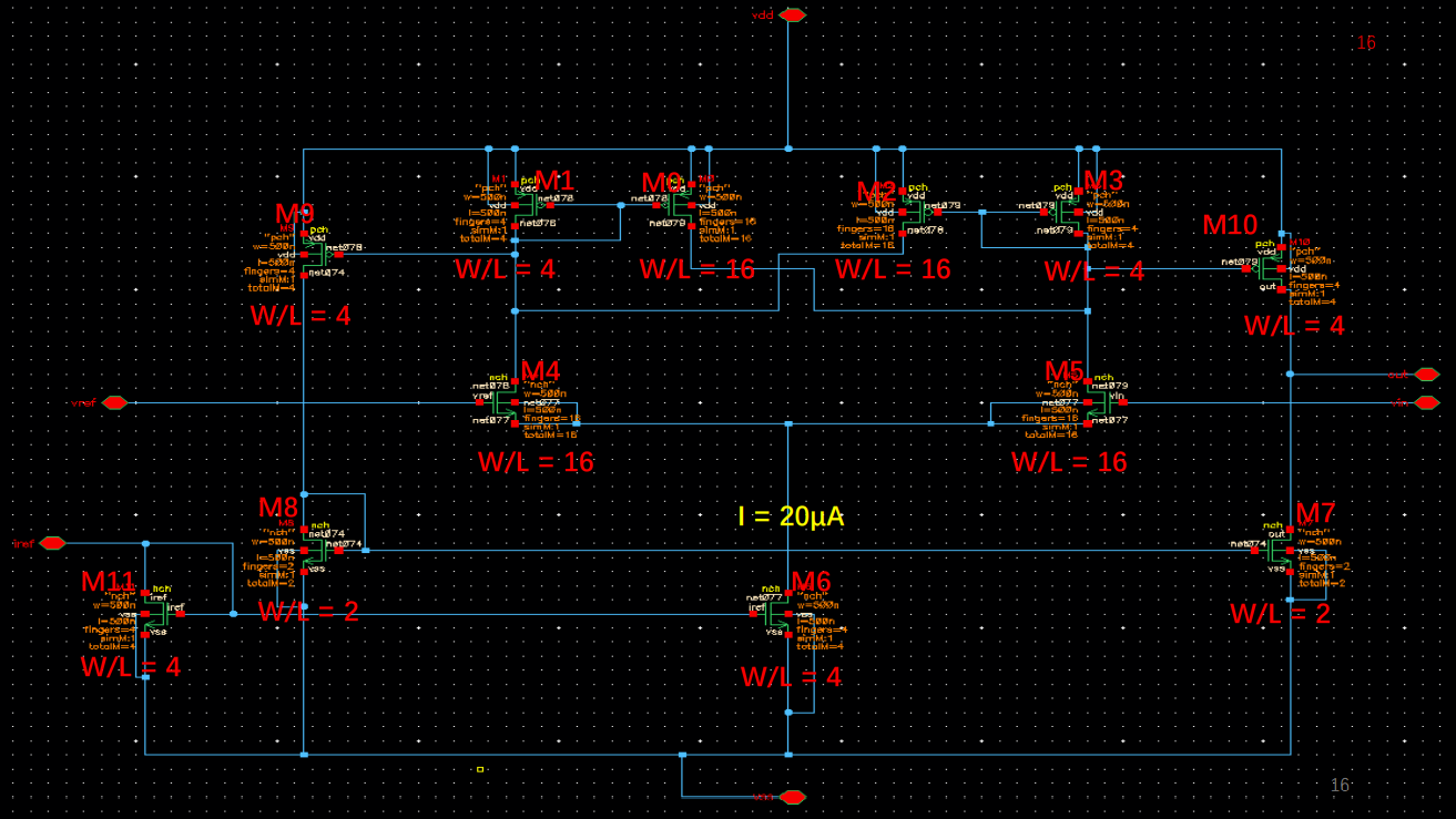
Fig. 7. Comparator Schematic
Fig. 8. 1 shows the specification of comparator. Fig. 8. 2 and Fig. 8. 3 proves that the designed comparator has correct function.
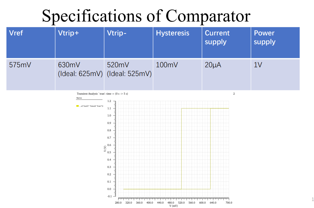
Fig. 8. 1. Comparator Specification
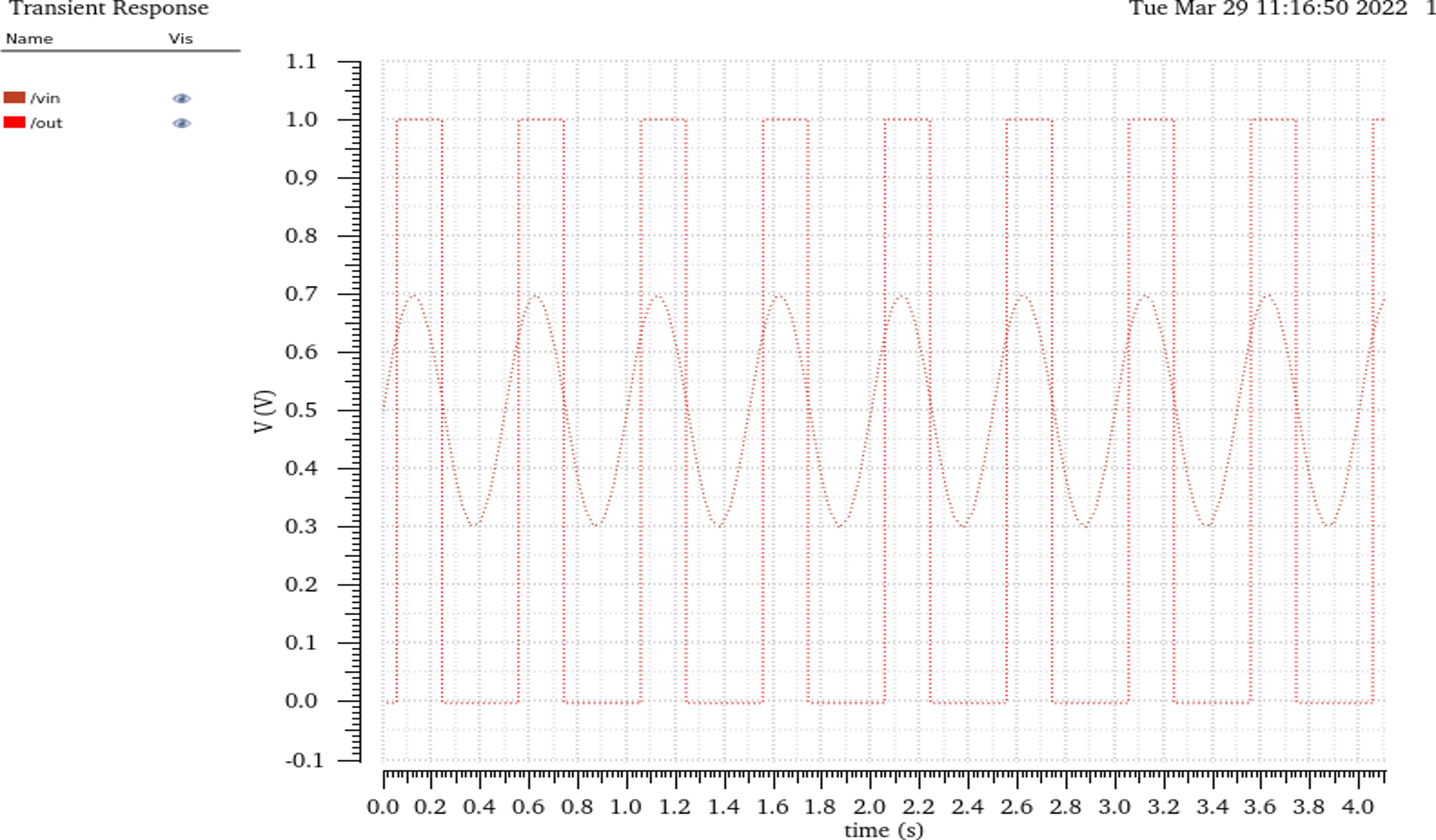
Fig. 8. 2. Comparator Transient Simulation Results
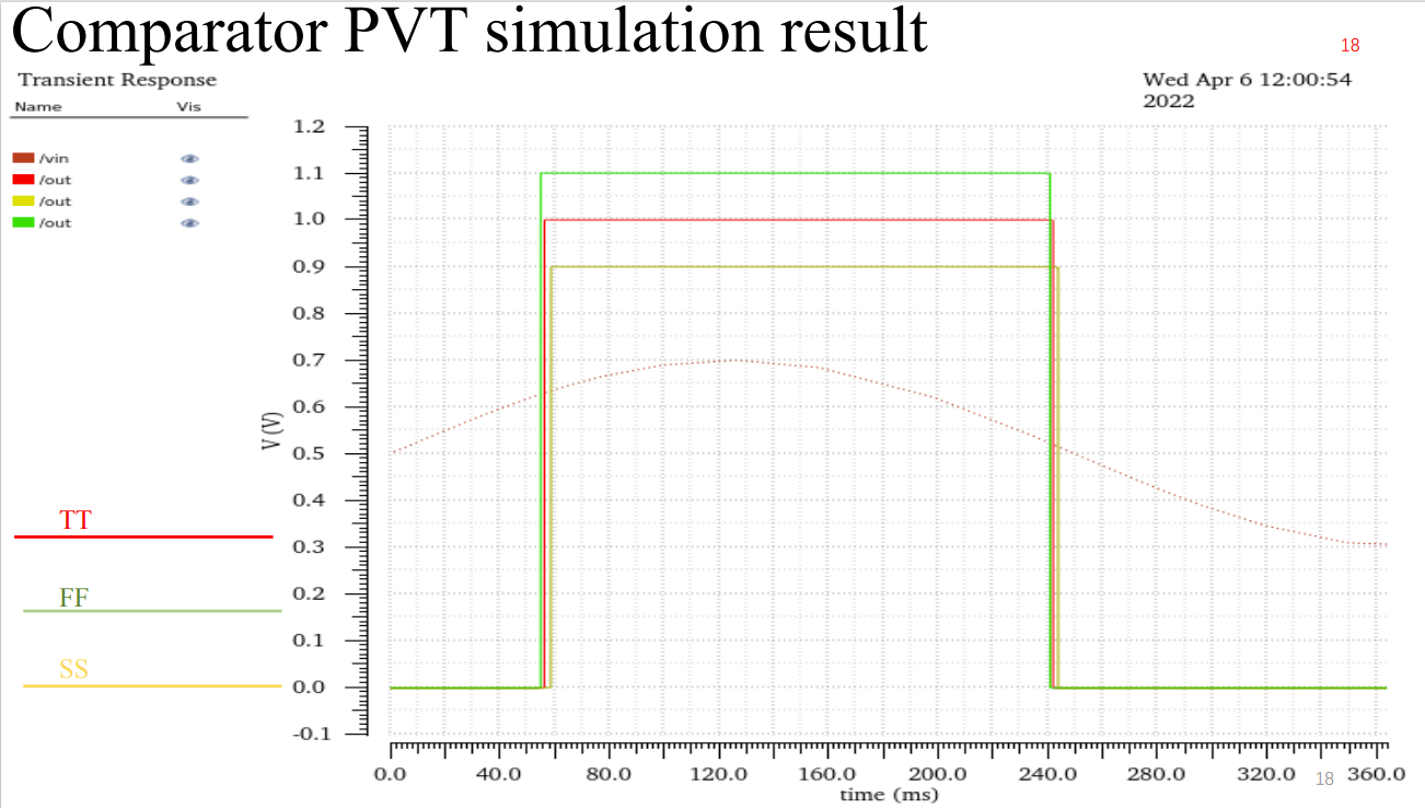
Fig. 8. 3. Comparator PVT Simulation Results