
Testing
Characterization of RF Band-Selection Filter
The S-parameter measurement for the RF band-selection filter is shown in Fig.1. From the graph, the input matching is very good across the FM band. The out-of-band rejection is high and the in-band insertion loss is 1.4dB.
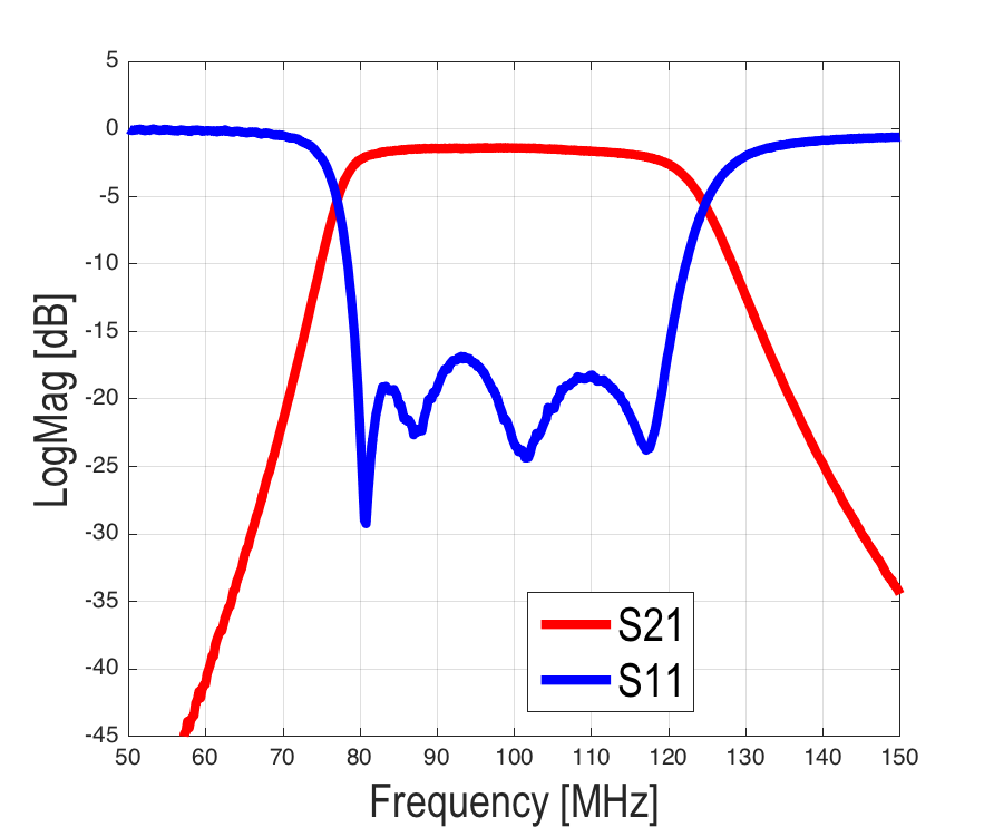
Fig.1 S-Parameter Measurement of RF Filter
Input Impedance of LNA
The S11 measurement for input impedance of the LNA is shown in Fig.2. The waveform is a little bit noisy, since we need to use a weak RF source signal in the network analyzer to avoid driving the LNA in saturation. At low frequency, the measured input resistance is , which is exactly what we designed for.
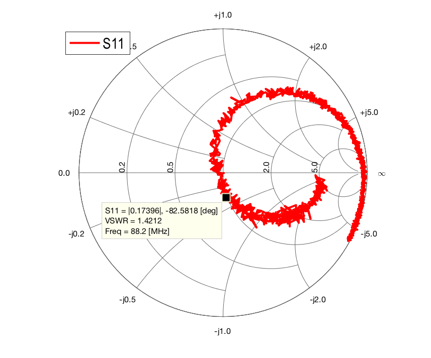
Fig.2 S11 Measurement at Input of LNA
Board Input Impedance
A two-element "L" matching network between the RF band-selection filter and the LNA is designed on the PCB using discrete components from Murata and Coilcraft. The S-parameter measurement result at the input of the matching network is shown in Fig.3. The input matching is below -10dB across the FM band.
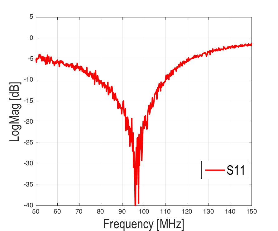
Fig.3 S11 Measurement at Input of RF Matching Network
Power Breakdown
The DC current consumption for each block is tabulated in Tab.1. The power consumption of the chip is below 1mW, which was the design target in the beginning of the project.
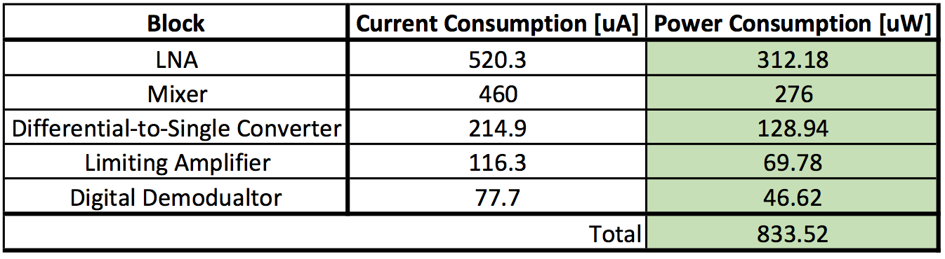
Tab.1 Power Breakdown
Front-End Conversion Gain Measurement
An HP8548A signal generator was used to generate a 1mVamp sine wave at 100MHz. By applying differential-LO signals at 110.7MHz, a 40.1mVapp IF signal at 10.7MHz is observed. Therefore, the RF front-end produces a conversion gain of 32.06dB.
Limiting Amplifier Voltage Gain Measurement
The limiting amplifier is used to rectify the small IF signals to rail-to-rail signals, such that the backend circuits can demodulate the FM signals. An HP8648A signal generator was employed to generate a -60dBm sine wave at 10.7MHz. A Keysight DSO1052B oscilloscope is used to observe that there is a 0.304V differential voltage amplitude at the output of the limiting amplifier. Therefore, the limiting amplifier produces a 54dB open-loop voltage gain, which is close to the post-layout simulation results.