
IC Layout
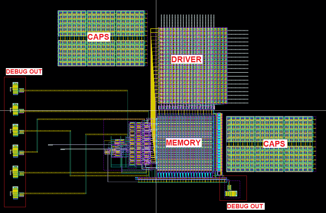
The active area used by the IC is approximately 0.64mm x 0.45mm. Figure 1 shows the overall layout of the entire IC. For high current routes such as VDDs, GNDs, and row and column driver outputs, multiple metal layers are strapped together. VDD and GND nets are laid out in a grid covering all active areas of the chip. Because of the relatively low clock speed requirement and loose tolerances for skew, no clock trees have been included in the design, but clock buffers have been included for each block. In total, there are 6 VDD connections from 6 VDD pins and 8 GND connections from 8 GND pins distributed across the IC.

Figure 2 shows the overall placement of all of the blocks which make up the IC. The memory array forms the core of the chip in the center. Below the memory sits the input shift register and latches and buffers for writing data. To the right, the decoders for row selection are laid out. Above the memory are the row and column drivers. In the left portion of the chip is where we find the logic for generating the PWM signal and ring counter. Decoupling capacitors are placed on two corners to improve robustness against transient variations in VDD. The total decoupling capacitance is 3.2 pf. Large buffers for debug and test points are placed near the output pins.
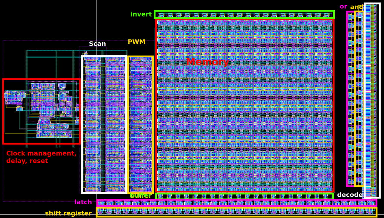
Final floor plan and placement of Reset, Scan, PWM, Serial Data, Decoder and Memory blocks is shown in Figure 3. The clock signal is buffered locally in every block.
The overall signal flow of the IC is shown in Figure 4.
