PCB Design
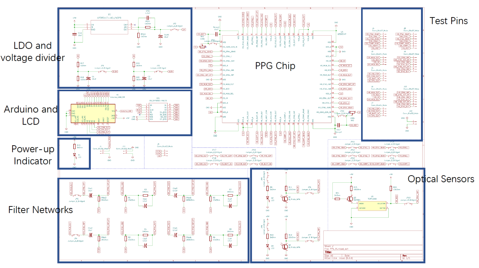
In order to verify the functionality of the chip and to connect the chip with other peripheral circuits, a 2-layer PCB was designed on the software KICAD. Fig.1. shows the whole schematic of the PCB. In the schematic, we decide to include these off-chip components in our system: an LDO, an Arduino Uno R3, an LCD, two voltage dividers, filter networks, optical sensors, test pins and a power-up indicator.

LDO & Voltage Dividers
By feeding the LDO with the 5V supplied by the Arduino, 1V power supply for the chip is generated. And these two voltage divider circuits are used for providing OTA bias voltage 0.5V and comparator reference voltage 0.6V. Fig.2. Shows these components on the schematic.

Filter Networks
The filter networks shown in Fig.3. are composed of LPF and HPF. They can help to filter the noise in the detected heartbeat rate signal from optical sensors.

Optical Sensors
There are two types of optical sensors used in our system (Fig.4.): The transmissive optical sensor and the Reflective optical sensor. The principle of these sensors is the same. And the only difference is the path of the light. For a transmissive optical sensor, the light will travel through the human’s finger to the phototransistors. For a reflective optical sensor, the light will be reflected by the phototransistors when it hit a human’s finger.

Arduino Uno R3 & LCD
We use Arduino to process the output signal of the chip and to get the heartbeat rate and the magnitude of oxygen saturation. The results will be displayed by the LCD components. Fig.5. shows the schematic.


