Circuit Design
The main building blocks of our chip are operational amplifiers (OTA), comparators and filters. The schematic of the whole system is shown in the figure below.
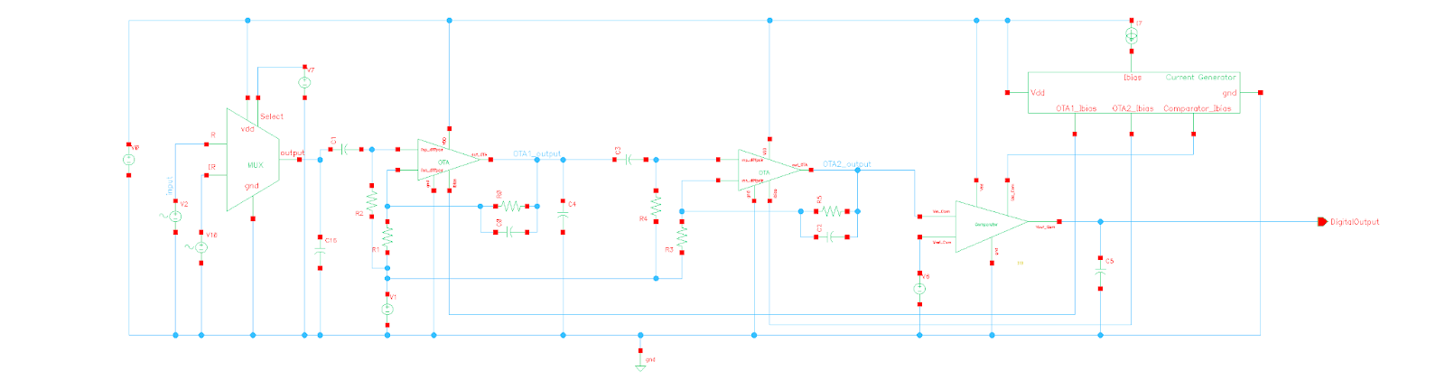
The input signal first goes through a first-order CR high-pass filter with a cut-off frequency of 0.5 Hz, attenuating the low-frequency signal. Then the signal goes into the first stage amplifier, whose closed-loop DC gain is set to 36.5 dB. The low pass filter with a cut-off frequency of 4Hz is implemented in the negative feedback network around the OTA. The output signal of the first OTA goes into the second OTA, which contains the same high pass filter and low pass filter as the first OTA. Then, the output signal of the second stage OTA which is also the analog output signal feeds into the comparator which functions as 1-bit ADC to get digital output. Finally, both the analog output and the digital output are sent to the Arduino board to deal with heart rate and blood oxygen level. The simulation result is shown in the figure below.
Block Design
OTA Design
For the OTA, we use a two-stage configuration with Miller compensation in between. The first stage is differential pair with active load, and the second stage is a common source. We decide to use the PMOS differential pair as input to decrease the noise of our OTA. The first stage is designed to provide high gain, and the second stage is used to increase output swing, which is from Vov to VDD-Vov. The schematic of our OTA is shown in the figure below.
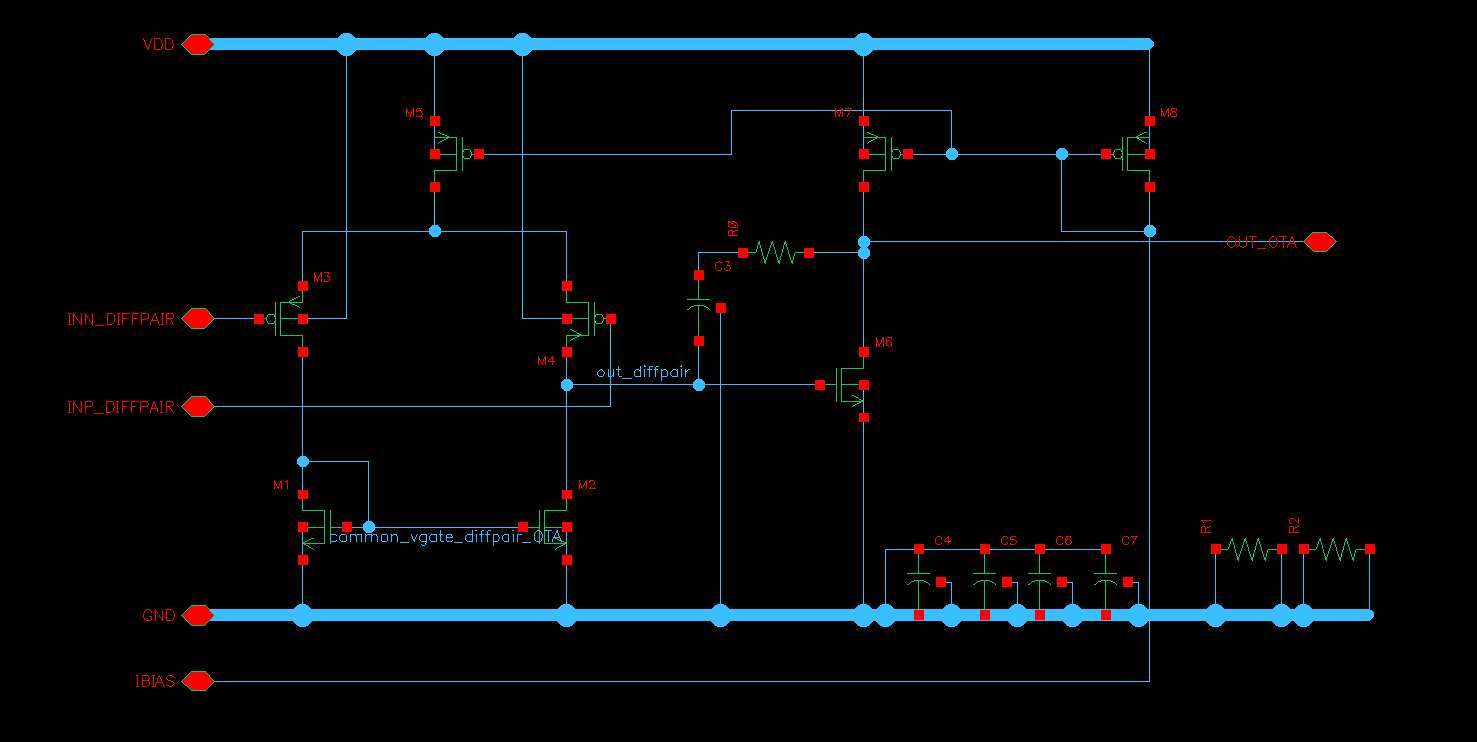
The reference current for the OTA is 20uA. The first stage current is designed to 20uA and the second stage current is designed to 40uA. Other simulation results are shown in the table below:
.png)
.png)
.png)
.png)
| Simulations Results |
Values |
|---|---|
| Reference Current |
20uA |
| Open-loop Gain |
60dB |
| 1st Pole |
9kHz |
| Linear Input Range |
-12mV ~ 12mV |
| Closed-loop Gain |
34.5dB |
| Closed-loop 3db Bandwidth |
0.42Hz ~ 4.57Hz |
| Phase Margin |
70° |
Comparator Design
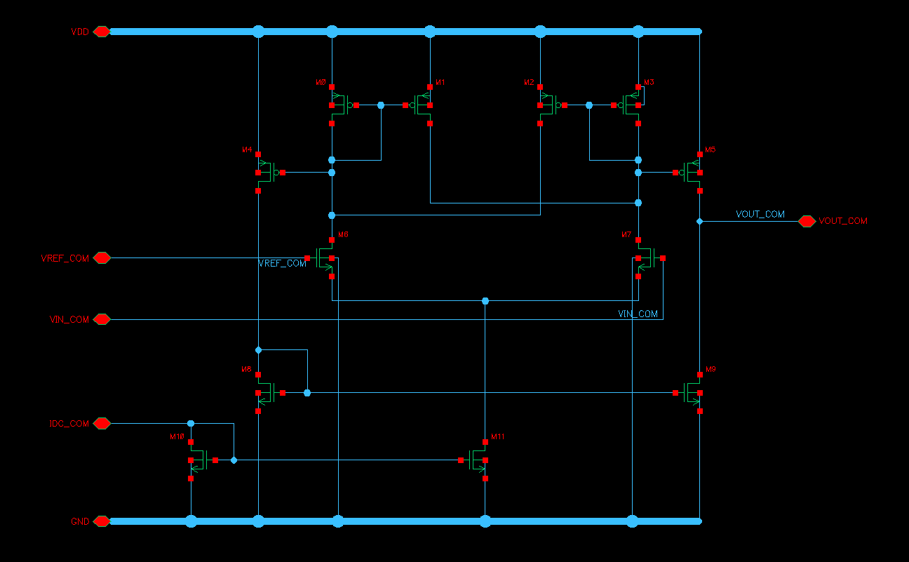
For the comparator, we use a cross-coupled structure as internal positive feedback to amplify the differential signal. This can help to suppress the influence of all kinds of noise in our application. The schematic of comparator is shown in figure below.
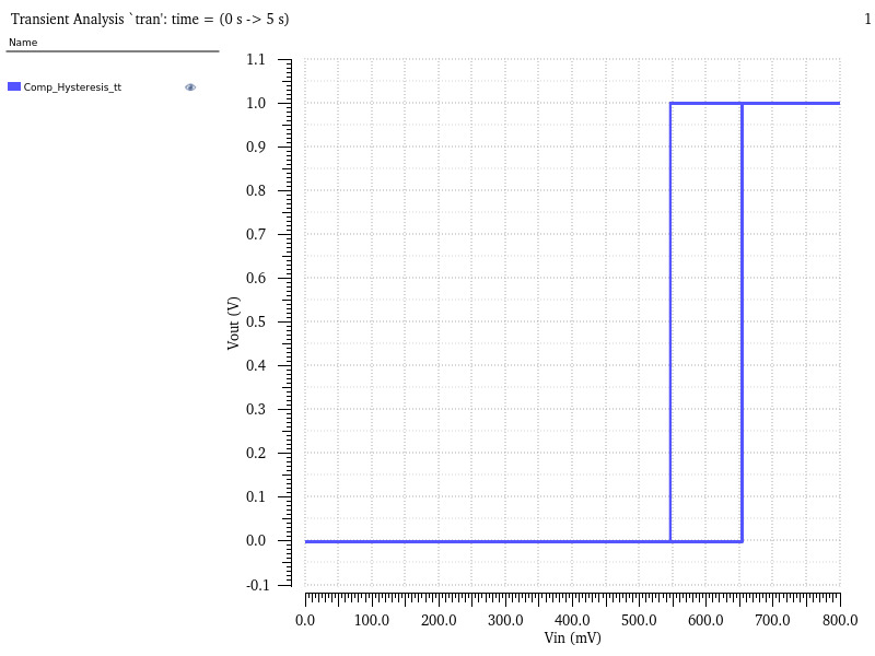
We apply a sine wave at the input of the comparator and set the reference voltage to 0.6V. The function verification simulation result is shown in the figure below. Since our system has a very low frequency, we do not care too much about the speed of the comparator. The hysteresis of the comparator is about 50mV across PVT simulation.