
IC Layout
For schematic and layout design we used Cadence Virtuoso CAD software, licensed to Columbia University.
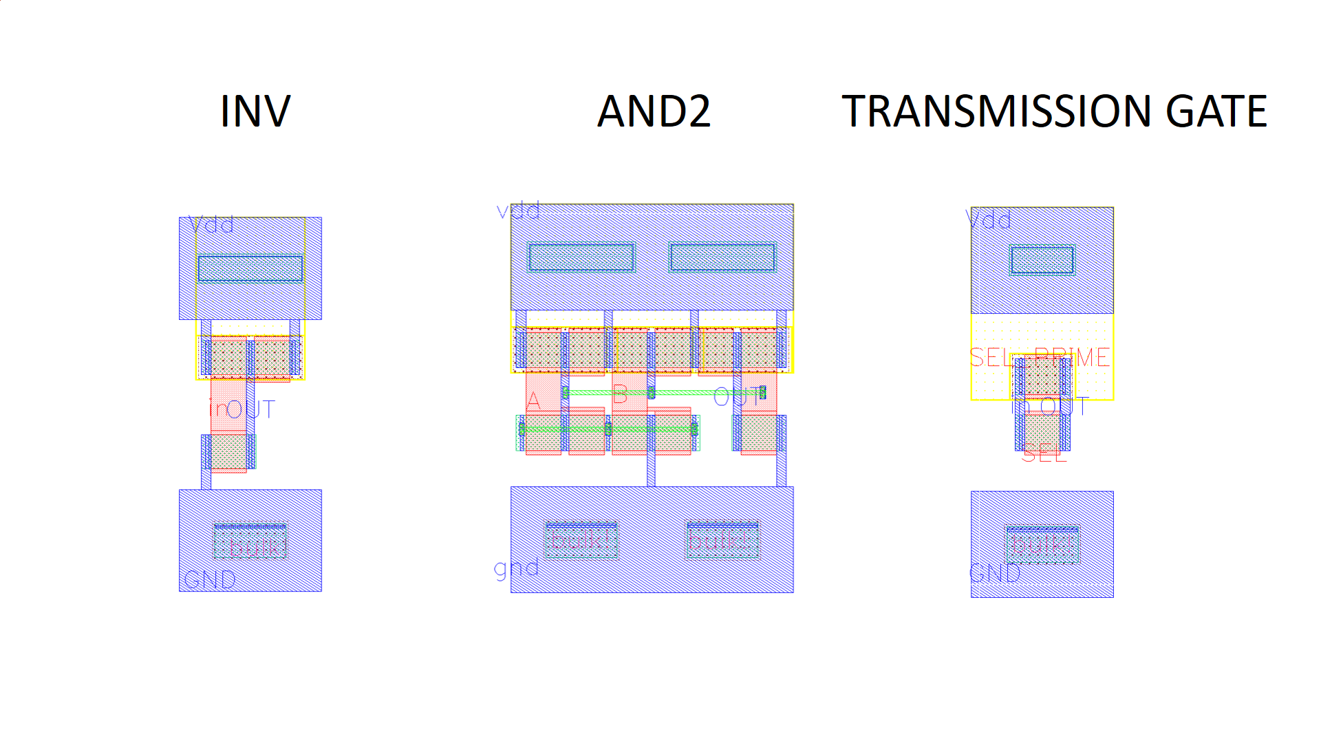
Fig. 9: Basic Cells - Finite basis of our design
We used CMOS VLSI technology and the basic cells - finite basis set we used for our schematic and layout were:
- INV
- 2NAND
- TRANSMISSION GATE
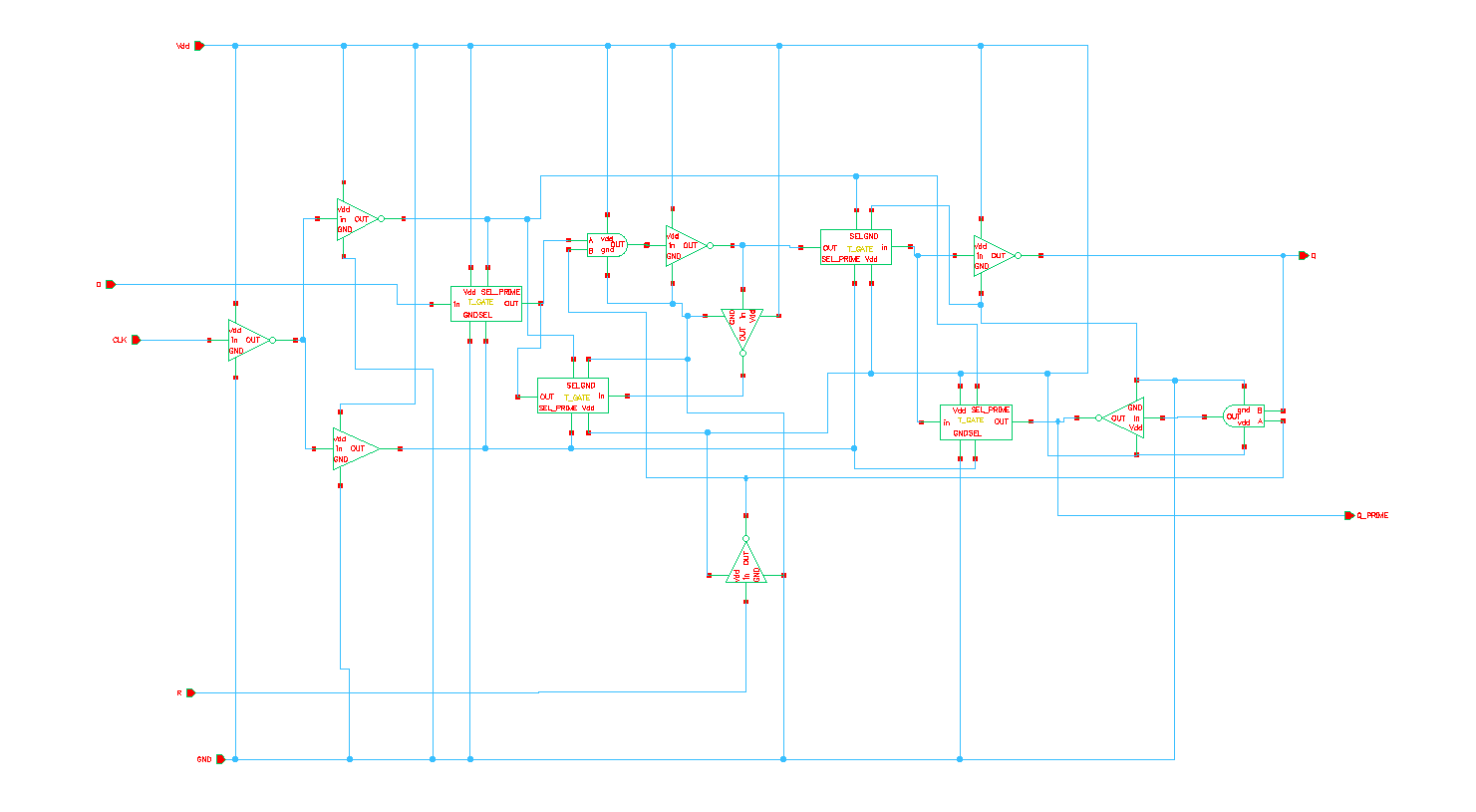
Fig. 10: D Flip Flop with reset schematic
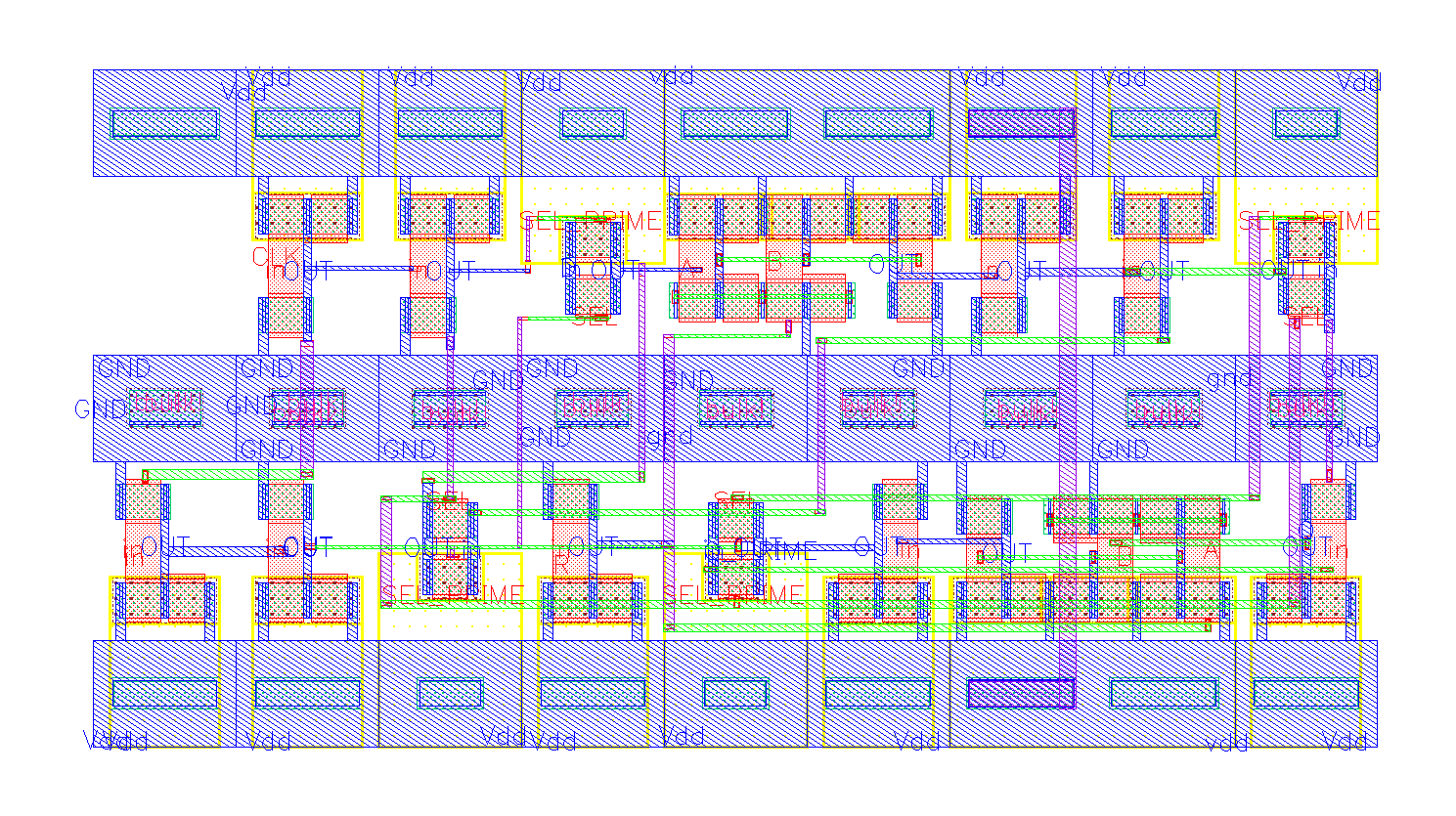
Fig. 11: D Flip Flop with reset layout
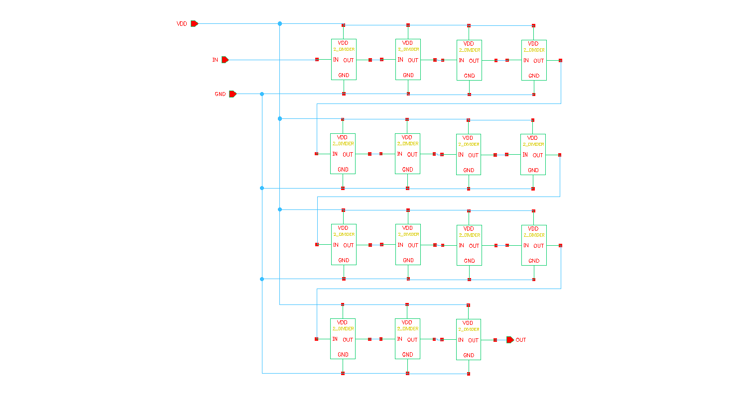
Fig. 12: Frequency divider chain schematic
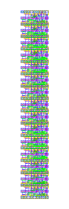
Fig. 13: Frequency divider chain layout
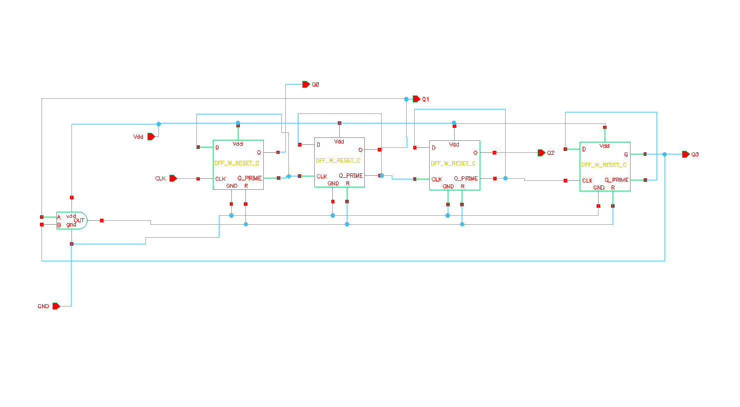
Fig. 14: Modulo 10 counter schematic
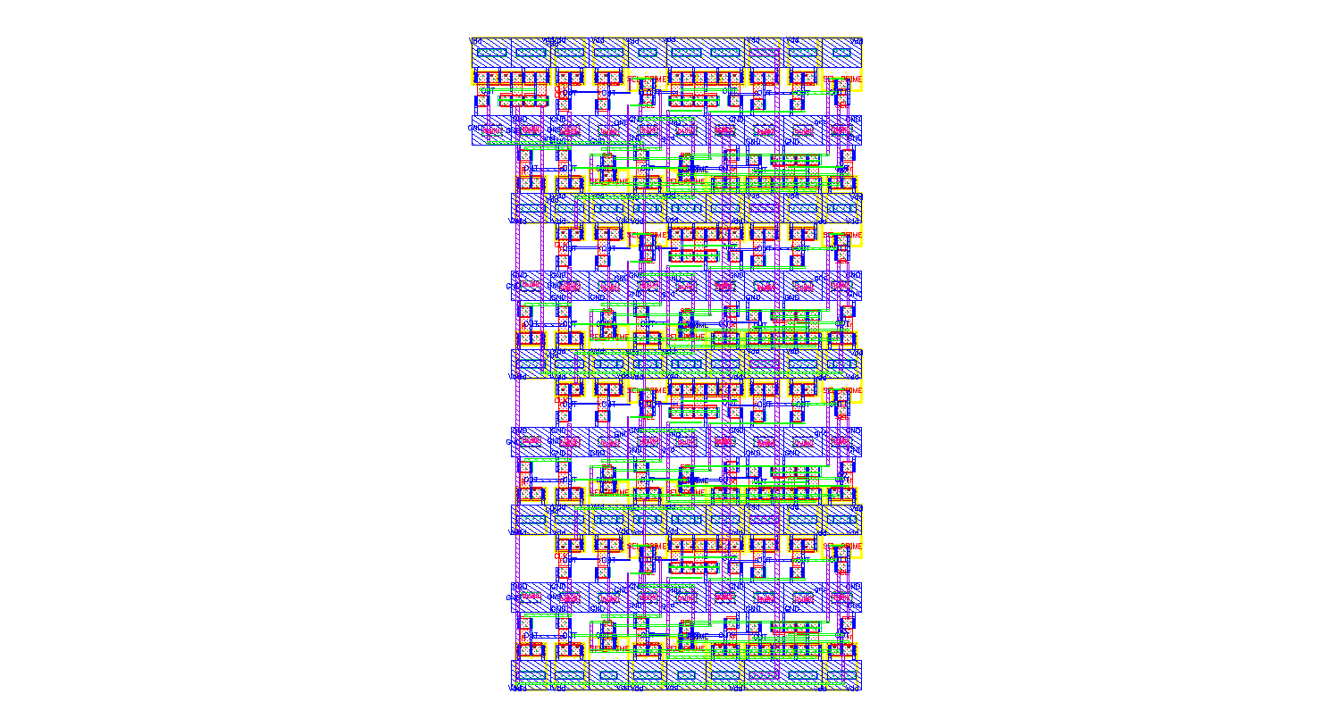
Fig. 15: Modulo 10 counter layout
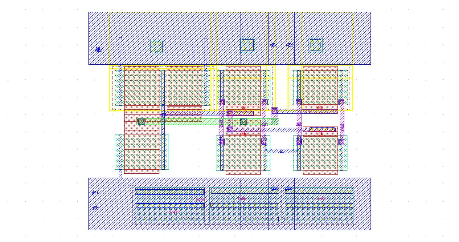
Fig. 16: 2x1 MUX Layout
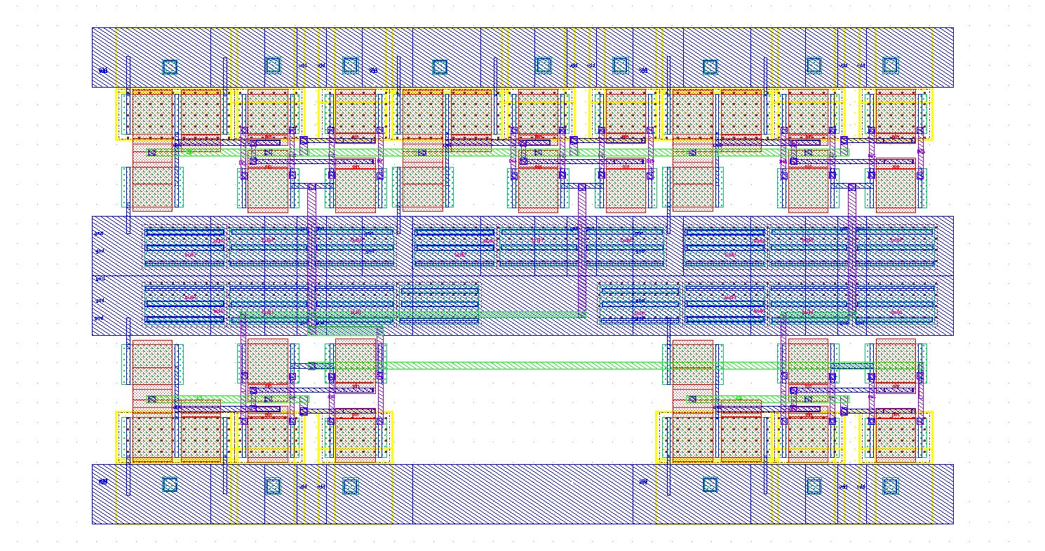
Fig. 17: 6x1 MUX Layout
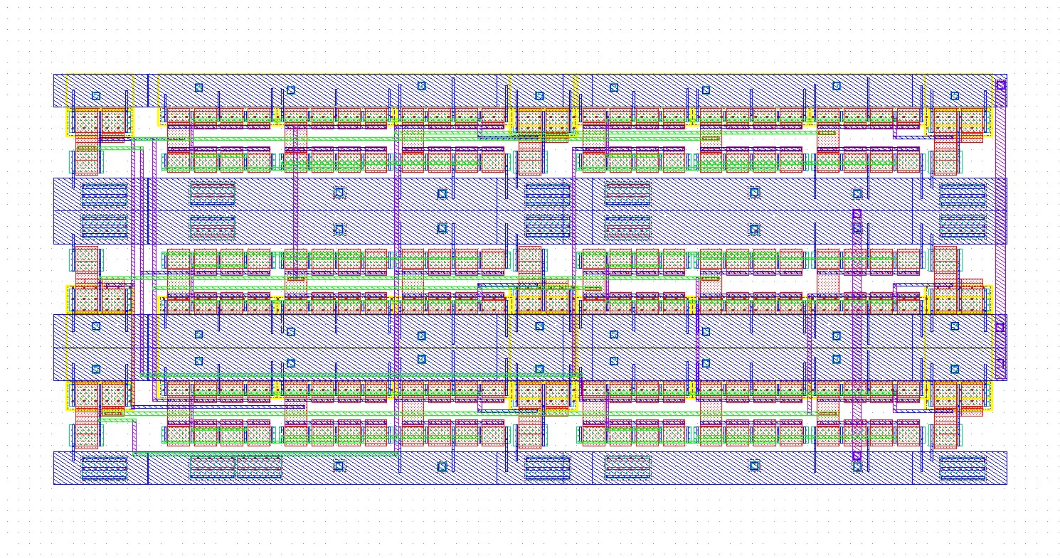
Fig. 18: 3x6 Decoder Layout
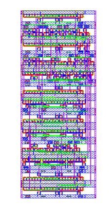
Fig. 19: 4x7 Decoder Layout
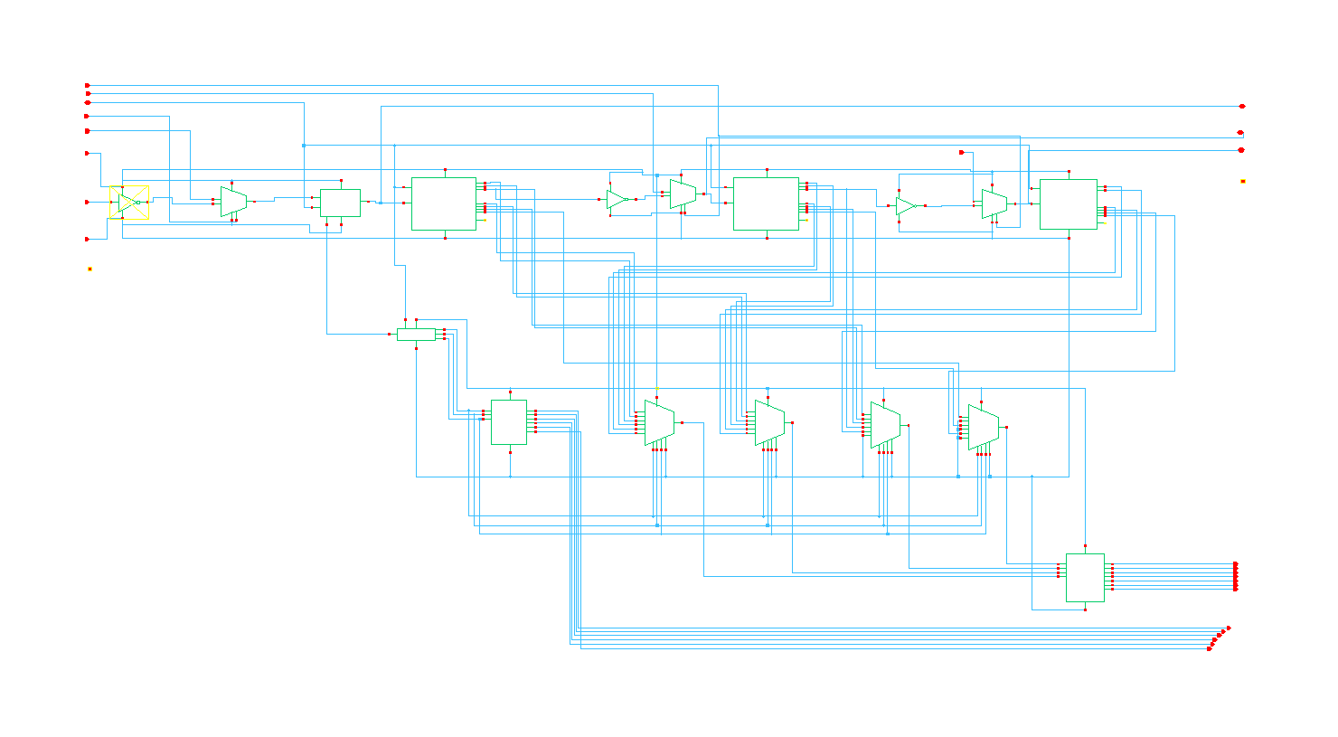
Fig. 20: Chip Schematic
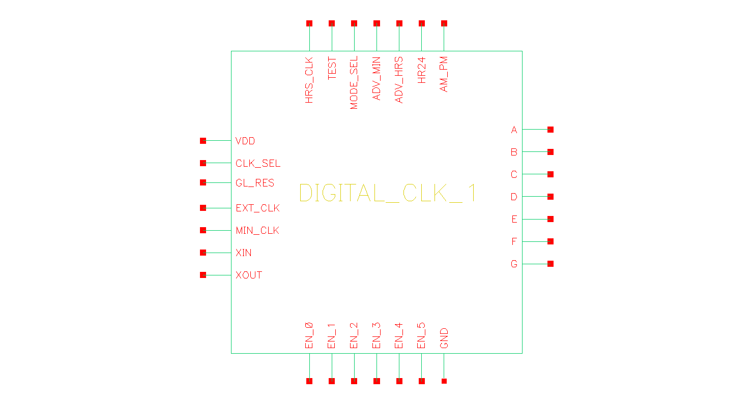
Fig. 21: Chip Symbol
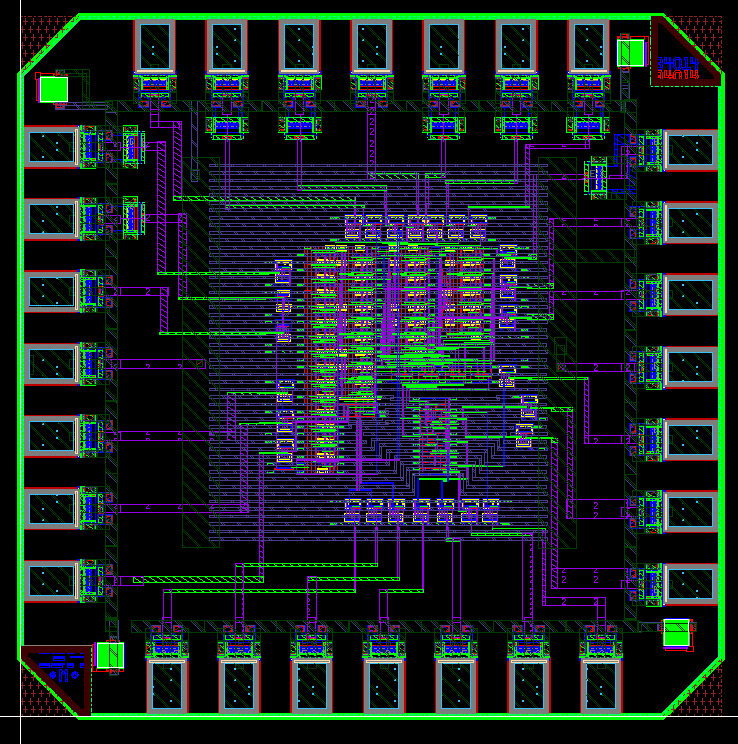
Fig. 22: Final Chip Layout