
Introduction
Welcome to the home page of the Digital Clock project for VLSI DESIGN LAB of Spring 2016 in Columbia University with Professor Peter Kinget. The fabrication of our chip was realized with the generous participation of the MOSIS educational program.
VLSI DESIGN LAB(ELEN 6350) is a project-based course that exposes students to an end-to-end product design. Every team is comprised of 2-4 students and selects a project to be produced. Students get the unique opportunity to deal with all the stages of a product design procedure.
These stages include:
- Defining application specifications
- Block diagram design of the chip
- Transistor-level schematic design & simulation
- Layout design & simulation
- Tape-out in accordance to MOSIS & IBM rules
- Chip-testing after fabrication
- PCB design
- Final Testing of integrated chip and PCB
- Detailed project report including webpage & video
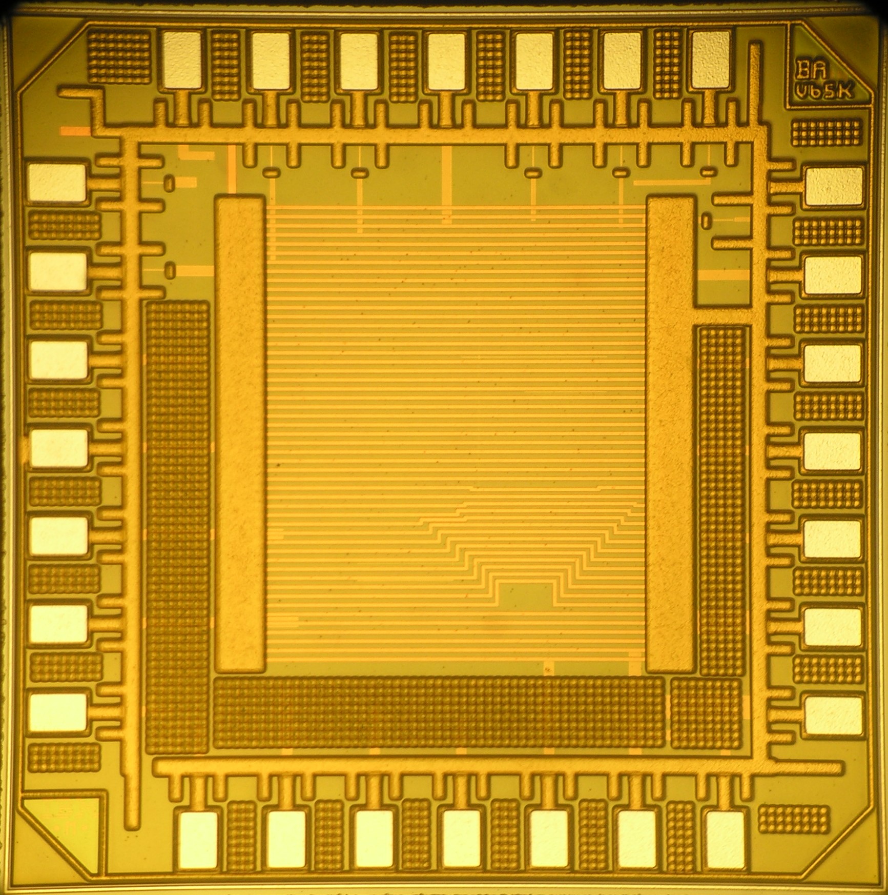
Fig. 1: Photo of the die
In this page you can find all the project related material and information. A digital clock project offers the student hands-on experience in digital design techniques like timing, encoding-decoding and logic verification but also establishes an analog approach as well.