System Design
The project is partitioned into two parts. The IC-chip handles all the digital logic computation, and PCB supports the I/O interfacing and peripherals.
IC Design
The top-level diagram of the chip is as shown below. It consists of a series of frequency dividers, one multiplex driver and a display decoder.
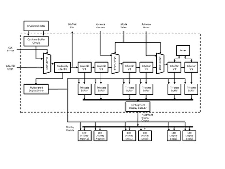
Apart from the user inputs and pins for settings, the IC chip takes an oscillation input from a crystal that resonates at 32,768 Hz. The oscillation is down-converted to 1 Hz through a frequency divider with a factor of 32,768. It feeds to the ones-digit of the second count, which feeds to the tens-digit of the second count, so on and so forth. For all ones-digits, the frequency divider is essentially a modulo-10 counter with overflow output toggling to the corresponding next-stage tens-digit frequency divider. The tens-digit uses a similar module-6 counter except for hours which uses a modulo-3 counter. Each digit's value is also output to a common bus in the format of BCD, binary coded decimal.
To display a digit on a 7-segment LED display, it requires a minimum of 7 control pins. To display 6 digits in parallel requires 56 control signals. This number exceeds the number of pins provided by a DIP28 IC packages. Hence, we used the method to time-multiplex some control signals, which reduced the number of control pins down to 13. We will be using the following multiplex driver circuit for driving the enable signals for the displays.