PCB Design
The most important consideration for the PCB design of an audio amplifier is ensuring that the power lines are routed carefully. Given the fact that the load is typically of the order of a few $\Omega$'s for audio amplifiers, any resistance in the power lines will appear in series with this and significantly affect power efficiency (and the amount of power delivered to the load). Therefore, the power lines on the PCB need to be made sufficiently wide so that their resistance is negligible (less than 1%) compared to the load resistance.
One of the implications of the filterless architecture is that the high frequency components at the output are not attenuated. Wires that carry these high frequency components will radiate these if the wires are sufficiently long. This radiation could interfere with other instruments nearby and can be considered to be a case of Electro-Magnetic Interference (EMI). The only way to mitigate this effect is to reduce the length of the wires connecting the chip to the speaker as much as possible.
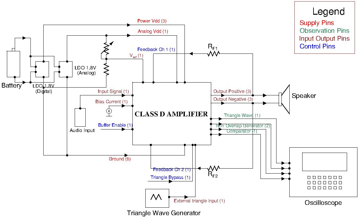
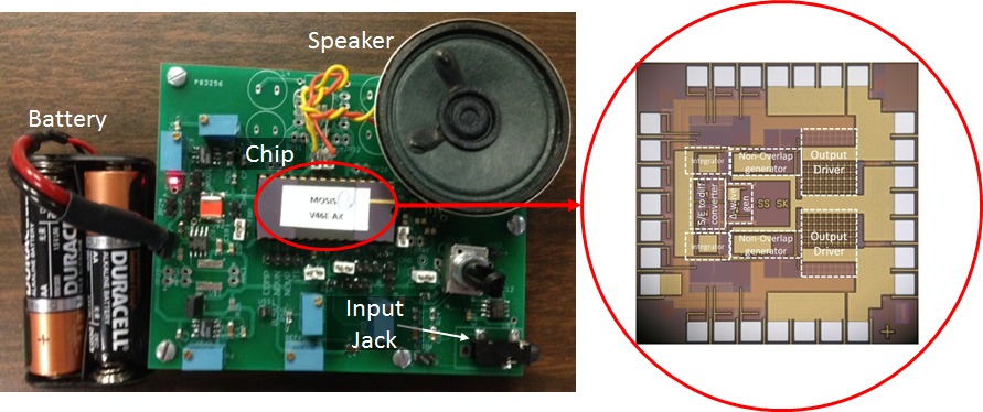
Figure 1 shows the block diagram of all the components on the PCB while Figure 2 shows the photo of the actual PCB annotated to show the most important parts.