Q: How do I find Noise Figure for the LNA?
Put a 'Vdc' source with 50 ohm resistance at the input. Simulate the total output noise using noise. Simulate the ac gain from the source to the output. Calculate the NF = (total noise at the output at the specfied frequency/ Gain*noise from source resistor(4kTR)).You need to do to AC simulation. See midterm solution as well.
Q: How do I simulate s-parameters?
For the project you only need to find S11. The reverse isolation has already been defined in terms of voltage (see the FAQ for the project). S21, S12, S22 are not useful for the LNA circuit you are designing since the LNA is driving a capacitive load not a 50 ohm impedance!To find the S11 parameter. Put a Vdc source (with 0 V dc and 1 V ac amplitude) with 50 Ohm source impedance at the input. Do an AC simulation; S11 can be calculated from the (complex) voltage at the input. In general, s-parameters can be found out as follows: Put a Vdc source with 50 Ohm source impedance at the input. Put a Vdc source with 50 Ohm source impedance at the output. Set ac amplitude in each source to be 1 V.
1) Turn on the input source; output source off; do an AC simulation;
S11 can be calculated from the (complex) voltage at the input;
S12 can be calculated from the voltage at the output.
2) Turn on the output source; input source off; do an AC simulation;
S22 and S21 can be calculated.
See section 4.3 (The Scattering Matrix) of Microwave Network Analysis, Second Edition, by David Pozar to know how to convert small signal Z-parameters to S-parameters
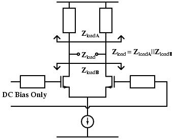
Q: How to find the output impedance of the LNA?
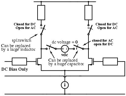
Figures below shows how to find the output impedance of the LNA. Our main problem here is to have a model for the output impedance.The output impedance of the LNA (Zload) can be decomposed into two parts - ZloadA and ZloadB. ZloadA is due to the load of the LNA --- this you know in terms of R, L and C. You need to measure ZloadB without affecting the circuit in any possible way.
We expect ZloadB to be a parallel combination of R(=1/g) and C (YloadB = g + jwC). Therefore, by putting a Voltage test source and finding the real and imaginary part of the current through the source, we can model the output impedance of the differential amplifier. Earlier I had mentioned putting a Current test source and finding the voltage across the source. Modeling the R and C using the voltage will be difficult (figure out 'why?').
In order not to effect the DC bias of the LNA, put a sp1tswitch in series with the vdc source (AC amplitude = 1, DC voltage = 0) and then do an ac simulation. If you do not have the sp1tswitch then you can replace them with large inductors. Real part will give the resistance and imaginary part should be dominated by the capacitance. This analysis did not include the capacitive load due to Mixer stage.