IC Design
Low-noise Amplifier (LNA)
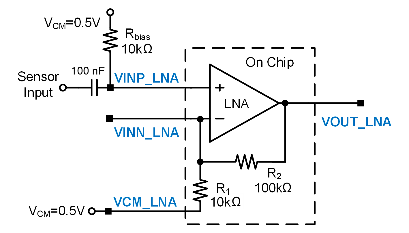
LNA is the first stage in the voltage-based sensor signal processing chain. The main requirements for this block are low input-referred noise, high enough voltage gain to reduce the system input-referred noise, and enough bandwidth to support the input frequency of the ultrasonic sensor. We implemented a low input-referred 2 stage Miller OTA in a closed-loop non-inverting amplifier configuration as shown in Fig. 1 and 2 below
Charge Amplifier (CA)
The input stage for the current based sensors is a charge amplifier. A charge amplifier is commonly used to interface with piezoelectric devices and acts as a current integrator. Using a feedback capacitor, an output voltage is generated.
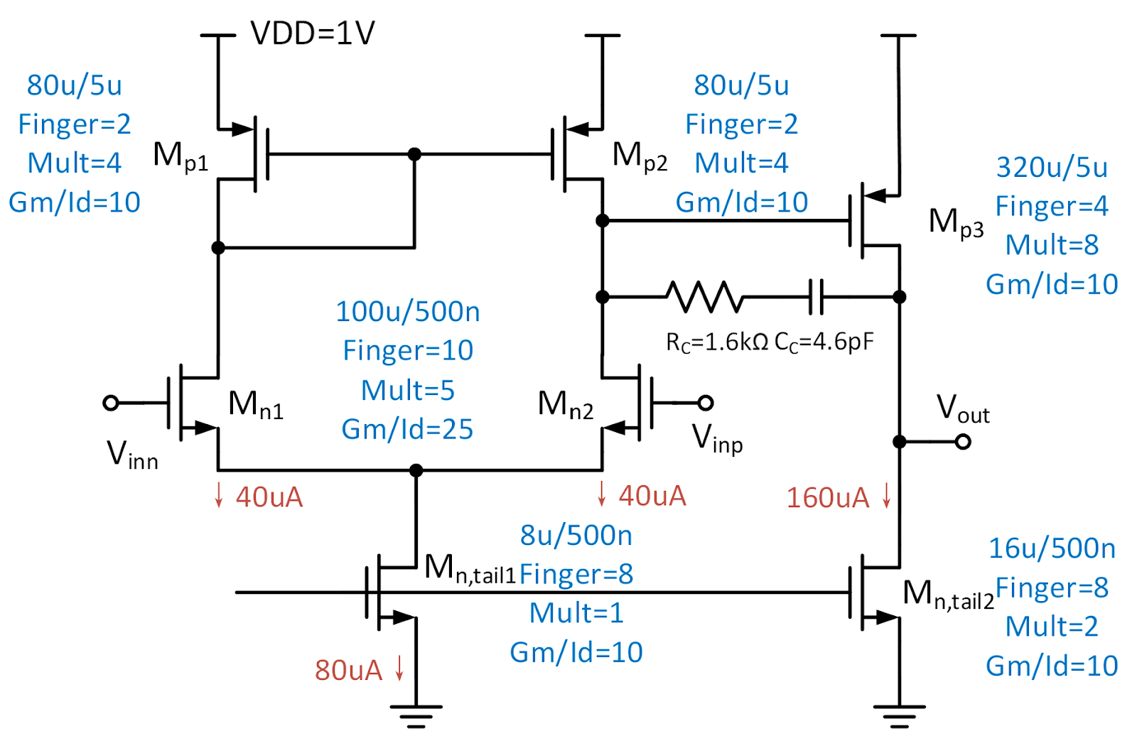
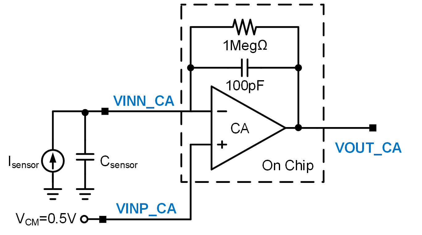
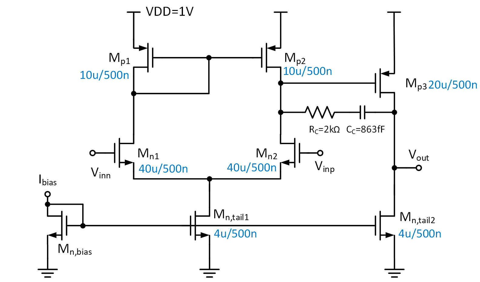
The schematic for the input charge amplifier is shown below in Figure 3. In this circuit, the circuit model for a piezoelectric sensor is attached to the inverting input of the amplifier. For this chip, the amplifier was realized with a two-stage miller opamp, which is shown in Fig. 4.
Analog Multiplexer
Since there are two sensor inputs, a multiplexer (Mux) is used to differentiate the input signal and pass it through to the next blocks in the circuit. The mux was implemented with two transmission gates for each input and an inverter to generate the complementary select bit. An external digital control signal is used to select the input signal. If the control signal is high, the output from the Charge Amp would be passed to the next stage. Otherwise, if the input signal is low the output from the LNA would be passed to the next stage.
Single-Ended to Differential Converter
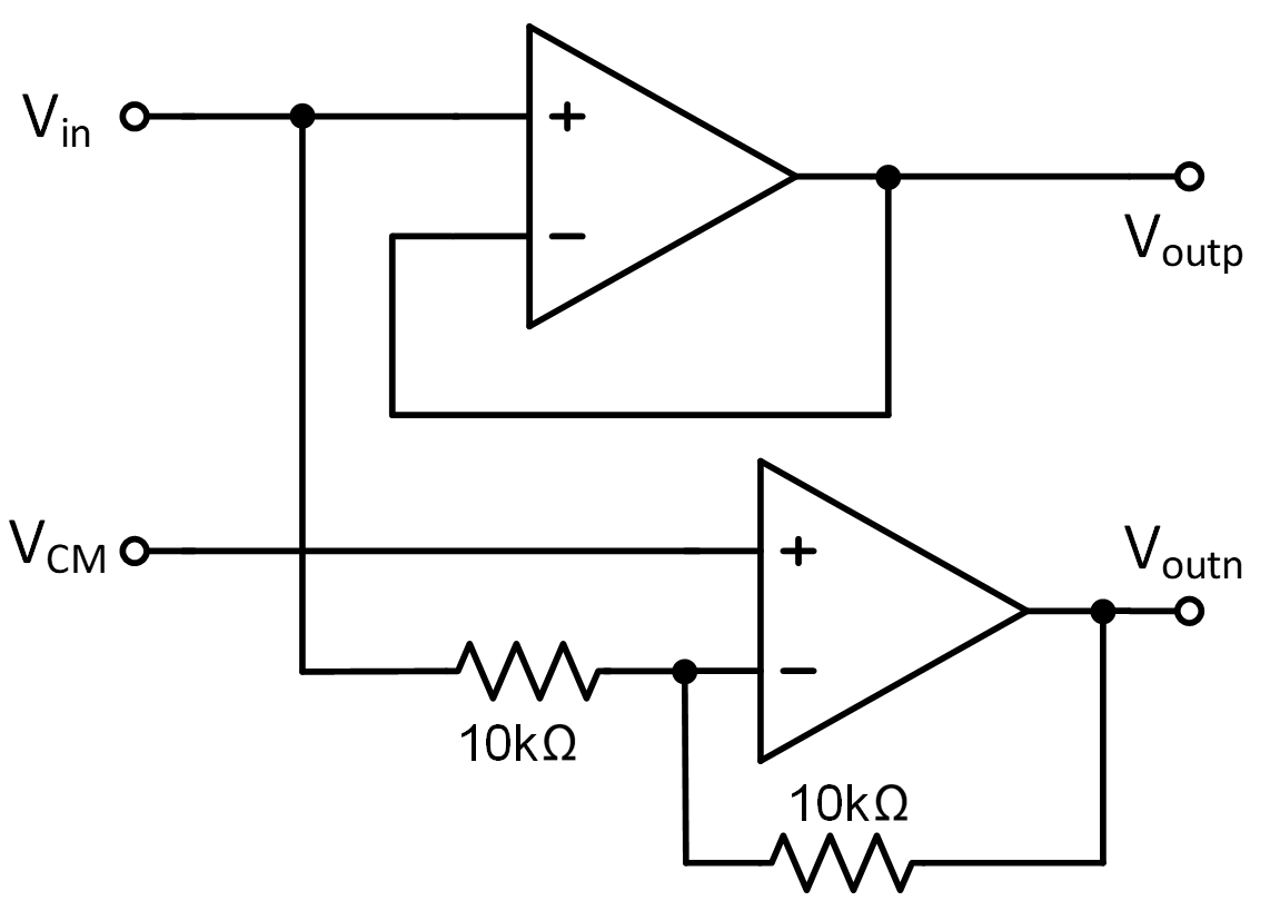
In general, differential signals offer a larger signal swing and immunity to common mode noise. These are important characteristics when dealing with analog sensor outputs. The basic idea behind a single-ended to differential converter is to have the single-ended signal enter both a unity gain buffer and a unity gain inverting amplifier. The output signal is thus taken as the positive output of the unity gain buffer and the negative output at the inverting amplifier with a common-mode voltage set by the voltage on the inverting amplifier’s positive terminal.
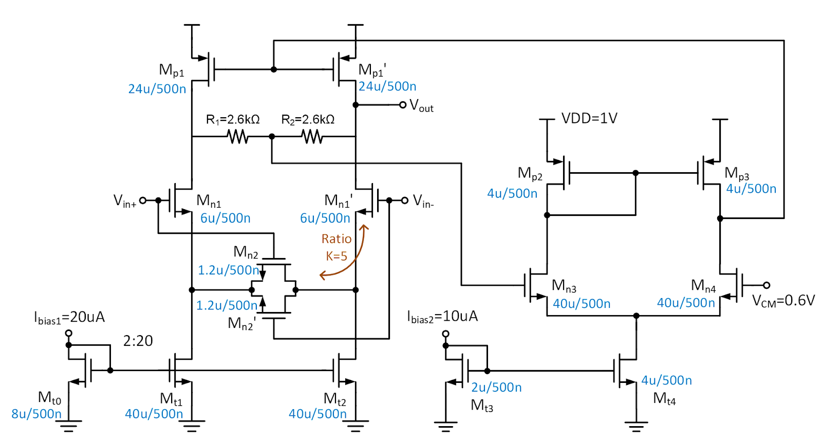
Programmable-Gain Amplifier
The programmable gain amplifier (PGA) consists of two stages of PGAs, as Fig. 6. shows. G[0:2] is the digital code that controls the voltage gain. For example, 000 gain setting has almost 0dB gain and 111 gain setting provides 34dB gain. For a single stage PGA, it includes a fully differential amplifier with resistive feedback and a replica circuit. The resistor ratio is controlled by the digital code. The replica circuit sets the output common mode voltage to VDD/2.
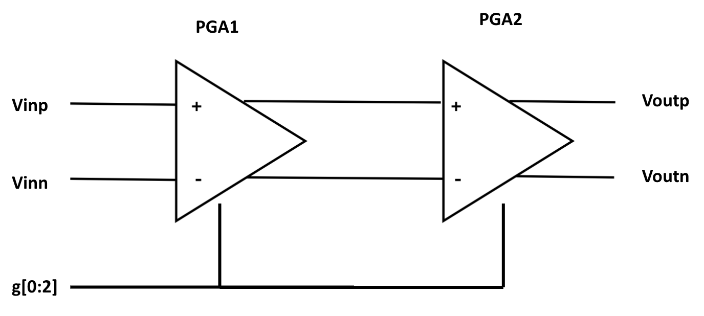
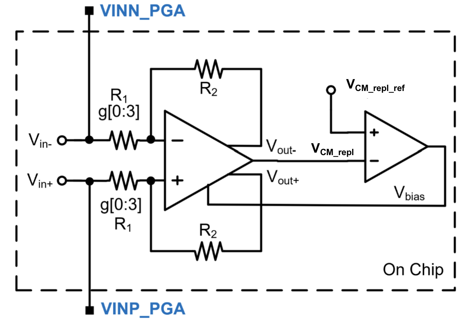
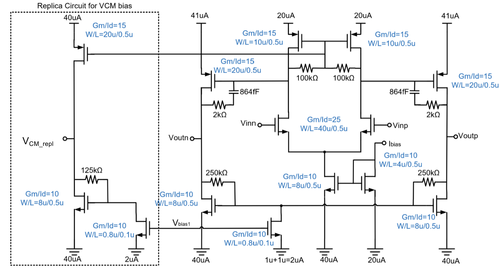
Table 1 below shows the digital code and its equivalent gain setting
| Digital code | Gain (ff,100deg,1.1V) | Gain (tt,25deg,1V) | Gain (ss,0deg,0.9V) |
|---|---|---|---|
| 000 | -300mdB | -100mdB | -130mdB |
| 001 | 26.8dB | 27.1dB | 27.3dB |
| 010 | 20.9dB | 21dB | 21.2dB |
| 011 | 33.1dB | 33.5dB | 34.6dB |
| 100 | 9.67dB | 9.72dB | 9.78dB |
| 101 | 28.9dB | 29.3dB | 29.5dB |
| 110 | 24.2dB | 24.4dB | 24.5dB |
| 111 | 33.7dB | 34.3dB | 34.6dB |
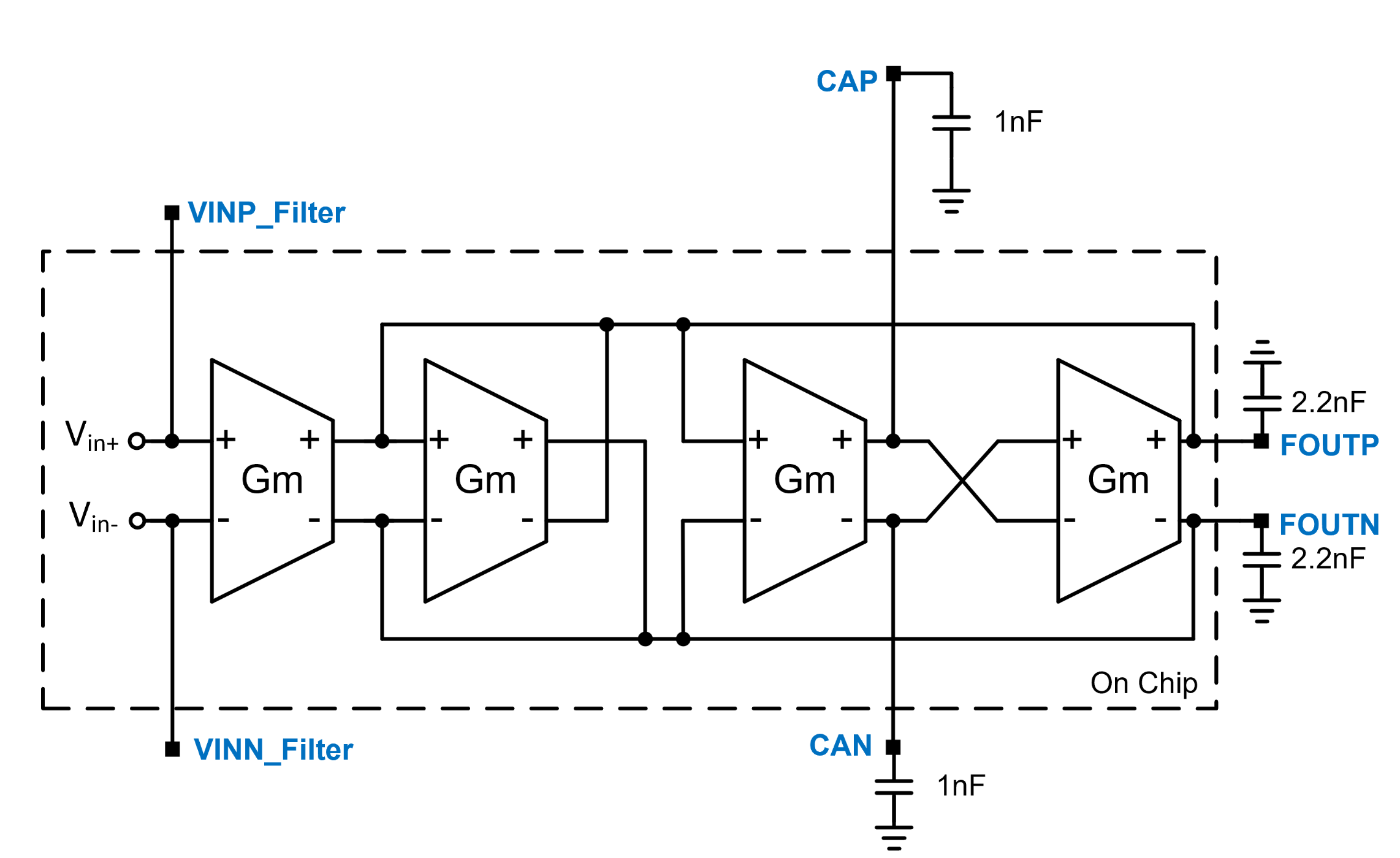
Filter
As the last stage of the Analog-Front-End, a fully-differential 2nd order GMC filter is applied to remove the high frequency noise from the sensor. We adopted source degeneration to build the linear GM block to get constant GM over a wide input range, as shown in Fig. 9. The resistive common mode feedback loop in this block will tie the VCM at 0.6V to reach a more linear region for NMOS input pairs. The whole filter is shown in Fig. 10, which has a high-pass cut-off frequency at Gm/√(C1C2).
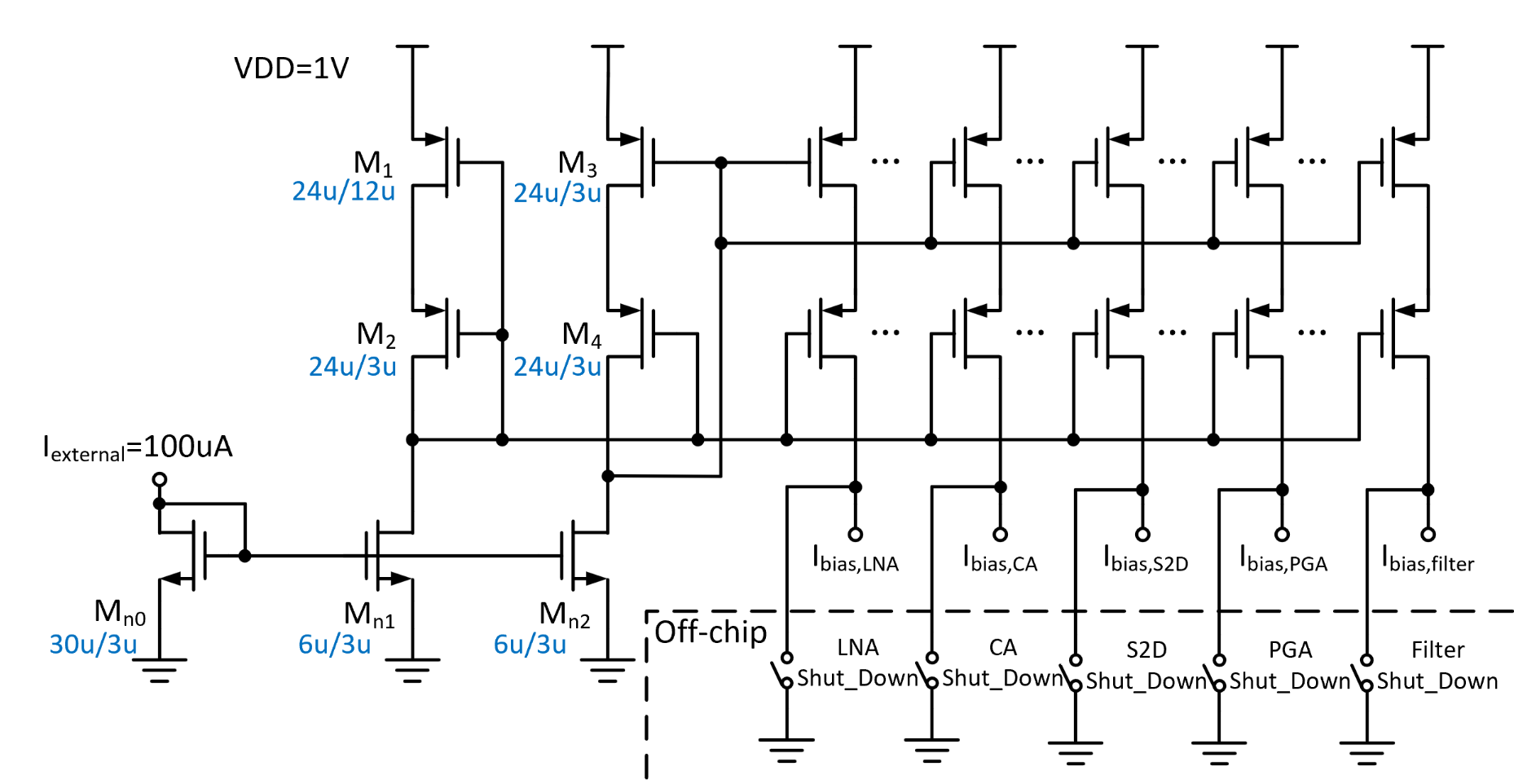
Current Distribution
Current distribution circuit in Fig. 11 will provide bias current for every analog block above, except the GM generator in filter, which needs off-chip tunable bias current to trim the process-dependent gm. With this block, only one bias current needs to be provided from off-chip and current routing, which will generate more accurate bias current than voltage routing, is available. For safety and convenience of testing, each bias point is connected outside that enables shutting down one block without affecting the operating point of the other block.