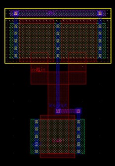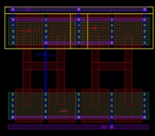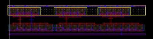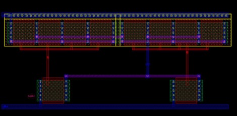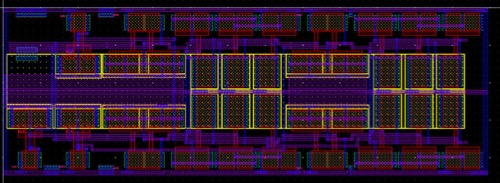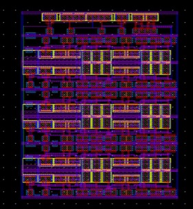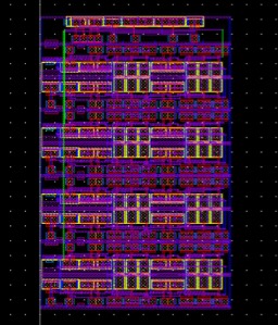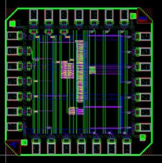
IC Layout
IC design and simulation was done using the Cadence Virtuoso CAD software, licensed to Columbia University Circuit and Embedded System Lab.
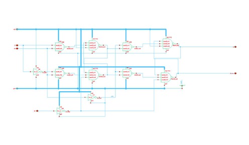
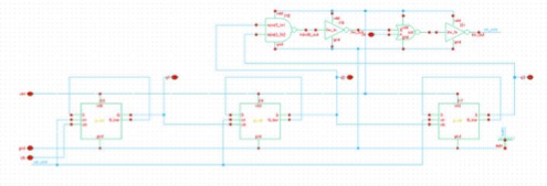
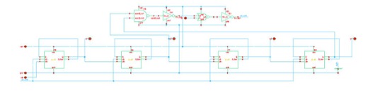
Basic Cells
For any digital circuit, we need a set of basic logic gates to implement its digital logic functions. These digital logic gates form a finite basis of all logic expressions. Some common finite basis are {AND2, OR2, INV}, {NAND2}, etc. Although the logic gates of a finite basis guarantee the completeness of all logic functions, it might not be an ideal circuit in terms of complexity, area, and power. Hence we implemented extra gates to accommodate a better design.We designed these digital logic gates using static logic family implementation, i.e. CMOS VLSI design style. In contrast to static logic family is the dynamic logic family, which normally implements faster logic gates using smaller area. However, the tradeoff of such design is complexity, which we avoided to guarantee a working final project.