LNA Design
Specifications
§ NF < 2.5 dB
§ Voltage Gain > 14 dB
§ Voltage Gain Variation over a channel (2.4 GHz to 2.423 GHz) < 0.2 dB at ‘tt’ process and 25°)
§ Fully Differential Circuit
§ IIP3 > -5dBm
§ Reverse Isolation > 25 dB @ 2450 MHz
§ Input Return Loss < -15 dB @ 2450 MHz
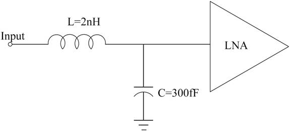
§ Assume the following interface to each input of the LNA: a 2mm bondwire (modeled as an inductor) and a bondpad (modeled as a pure capacitor).
§ Assume the LNA is driving 250 fF of capacitance. This capacitance is just an ad-hoc modeling of the LNA load which consists of the gate capacitance of the mixer stage and the parasitics associated with any coupling capacitor that you may use. This is just to help you start the design. When you put together the LNA and the mixer then you may need to modify the one and/or the other to get the specifications right and may be to get better performance.
You have to measure the input return loss under the condition of matched input impedance. The differential input resistance is 50 ohm at 2.45 GHz, thus first you have to match the differential impedance seen from input to 50 ohm at 2.45 GHz. Input return loss is defined as
20log|S11| dB
Simulations: The specifications given above are for ‘tt’ (typical, typical process) and 25°. You also have to simulate your design at typical, worst and best case corners. Fastest (best) case is -40C, ff process and 1.95 V. Worst case --- 85C, ss process, 1.65 V.
See FAQ for clarifications.
Submission: You have to submit the following materials on October 15th, 2005
§ Transistor level schematic of your design
§ Top-level schematics for all test setups. Create a symbol for your LNA and bring out all input, output, power supply and bias pins. Then create top-level test benches, and submit them with your design. You don’t have to submit the same schematic again and again since you are simulating for different corners or different temperature.
§ Simulation results at all temperatures and corners.
You don’t need to submit hardcopies, unless you have to or want to show any calculations. You can just e-mail the postscript files of schematics and simulation results. If you are working in a group, please cc your partner and put the name of your partner in the message.
Links
§ http://www.maxim-ic.com/quick_view2.cfm?qv_pk=2357