Frequently Asked
Questions
Q: What is reverse isolation?
A: For a 50 ohm system (input and output are matched to 50 ohm, your circuit is driving 50 ohm output), the reverse isolation is 20*log(|S12|). When the LNA is driving an on-chip capacitive load (input of a mixer), then the gains are defined in terms of voltages --- there is no power transferred to a capacitance. Similarly the reverse isolation needs to be defined in terms of the voltage that you see coming at the input terminals of the LNA when you apply a signal at the output terminals of the LNA --- just like when you try to characterise the output impedance of a circuit.
Q: What is the equation for the parasitic resistor in the inductor model?
A: In reality, the value of the parasitic resistor depends only on inductor value and layout structure. However, when we model the inductor, we define a Q value for a certain narrowband frequency range. The value of the Q depends on the value of inductor, the value of resistor and the frequency. In the given model, the Q of the inductor is defined as 7 for the 2.4 GHz ISM band. So, you can derive the value of the resistor for Q of 7 and frequency of 2.45 GHz. If you don’t know the equation for Q of an inductor, please check some textbooks (T. Lee: "The design of CMOS Radio-Frequency Integrated Circuits” ) or try to derive it by yourself.
Q: What is the load of LNA?
A: Since it is a quadrature receiver, the outputs of the LNA are connected to two mixers. You may check some 2.4 GHz receiver publications and have an idea about the transistor sizes of the mixer seen by the LNA outputs. Then you may have an approximate model for the load of LNA by putting some dummy devices at the outputs with appropriate sizes at the specific operating point. You may also model the load as a capacitor and find the approximate value of it by calculating the input capacitance of the transistors. If you can’t find any information about the transistor sizes of a 2.4 GHz ISM band mixer, you may use a replica of the input transistor of your LNA as the load of your LNA.
Q: What is the input interface of the LNA?
A: For the LNA design, please use the following input interface in your simulations.
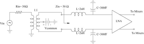
The BALUN shown in the diagram is
an ideal 1:1 BALUN.
First note: looking into the Balun Primary you want 50 ohms. Looking into the differential input of the LNA you want 50 ohm impedance since you are given a 1:1 Balun. So each side of the differential LNA needs to be 25 ohms.
The bondwire inductance and bondpad capacitance needs to be included in the design. That is what the interface shows. They have to be accounted for while designing for the input match. Your LNA cannot interact with the world without the bondwire or the bondpad.
You need 50 ohm input impedance when you are driving circuit from outside the chip .... LNA gets the input from outside the chip.... Mixer is not driven from off-the-chip. When you are designing and testing individual components - LNA, mixer... then you would need to design a matching network to get 50 ohm output and input impedances. Not here...
Q: What does LO = 300 mVpp and Power(RFIN)=-30dBm mean?
A: It is to measure the LO feedthrough to RFIN and IFOUT terminals under the assumption that there is 1% mismatch between the transistors of differential pairs, and under the condition when the LO voltage is 300mVpp and the RF input power is -30dBm.