
Introduction
Welcome to the Home Page of Digital Clock Group.
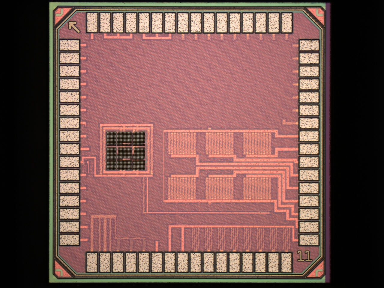
The chip design process is based on TSMC 65nm technology and the fabrication is generously sponsored by Apple Inc.
The basic desig process can be seperated into two parts, 1. Digital Core; 2. Analog Components.
For Digital Core, ASIC design flow is implemented including but not limited to 1. Chip Design Specification; 2. Architectural Design; 3.Behavioral Verification & Functional Simulation; 4. Logic Synthesis; 5. Post-Synthesis Simulation/Verification; 6. Place & Route; 7. Post-PnR Simulation/Verification.
For analog components, analog part mainly consist of level shifter for 1V to 2.5V, input/output buffers, and led/buzzer drivers. All those parts need to make sure the transfer time is small enough compare to our clock cycle, and the for the driver, we need make sure the driving capacitance of the current meet the offchip devices' need as well as make the driver on-resistance small enough.
The goal of this design is to accomplish three time mode display, 1. Clock Mode; 2. Date Mode; 3. Timer Mode.