
Introduction
The purpose of this project is to design a audio signal processing chip including a 10-bit Successive Approximation Register Analog-to-Digital Converter(SAR ADC) and a 10-bit R-2R Digital-to-Analog Converter(R-2R DAC). The sampling rate of ADC and DAC are 100k sample per second.
The area of the whole chip is 1mm2 and the supply voltage is 2.5V. The chip is demonstrated within the whole audio system. As you can see in the Figure. 1, the audio input comes from iPad and passes through audio jack, single ended input to differential output amplifier and anti-aliasing filter. The ADC would output 10-bit digital voltage results every 10 us. The FPGA or other microcontroller can receive these digital signals and make signal processing. The DAC would receive the output from the FPGA and feed into the class-d amplifier after a low-pass filter.
The effective number of bits (ENOB) of ADC is 7.5 bits and the value of SFDR is 51.39dB. The range of ADC is from 0 to 2.5V. The maximum DNL value is 0.99 LSB while the maximum value of INL is 2 LSB. For our 10 bit DAC, our output voltage range is 0.6-1.8V with a sampling rate of 100kHz. Its ENOB is approximately 8.5 bits, which varies with the input frequency. DNL maximum is 0.27 LSB, INL maximum is 1.5 LSB.

Figure 1: Block diagram of the Whole System
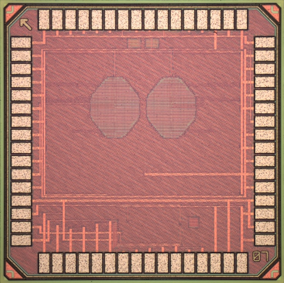
Figure 1b: 65nm CMOS chip photograph