
Systen Implementation
Transimpedance Amplifier
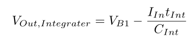
A current integrator scheme [1] was chosen as the first stage of the Transimpedance amplifier (see Fig. 4).

When the switch (connected to clock phi1) closes, the two terminals of the capacitor are shorted, and there will be no charge stored in the capacitor. The voltage seen from the terminal Iin is the same as VB1. When the switch opens, the input current would start to charge the capacitor. Since the operational amplifier (Opamp) (or a operational transconductance amplifier (OTA). For this specific case, it doesn't matter since the output resistance of the amplifier is always smaller than the resistive load it needs to drive, as all the loads should be capacitive) has a high voltage gain, the voltage at inverted input terminal won't change a lot, but the output voltage of the Opamp after integrating for time tint is:
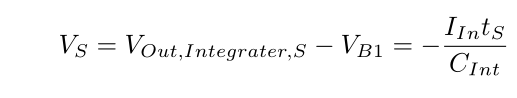
The first stage and the second stage are connected by a capacitor CS. When the second stage switch (connected to clock phi2) is closed, the sampling capacitor will sample a voltage VS at time tS, which is the difference between the output of the first stage and that of VB1:
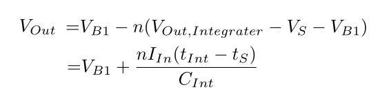
When this switch is opened, the summation of charge at the inverted input of the Opamp cannot change. Any further voltage change at the output of the first stage would induce an -n times change at the output of the second stage due to charge sharing between CS and the feedback capacitor CS/n. Since the output of the first stage is a summation of integrated current and the noise of the amplifier, the voltage at the output of the second stage at time tint would be:
The third stage is a sample and hold stage. When clock phi3 is high, the capacitor CT tracks the voltage at the output of the second stage. When phi3 is low, the charge is redistributed between CT and CT/m. This provides another m times gain at the output. And the final output voltage will be:
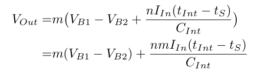
The product mn is called post integration gain. And adjusting VB2 could compensate some amount of DC components in IIn.
Rail-to-Rail-Input-Output Amplifier
In order to expand the voltage range as well as increasing the output swing of the transimpedance amplifier, a constant-gm constant-slew-rate rail-to-rail-input-output (RRIO) amplifier [3-6] was designed. The schematic is shown in Fig. 5 without bias circuitry for simplicity.
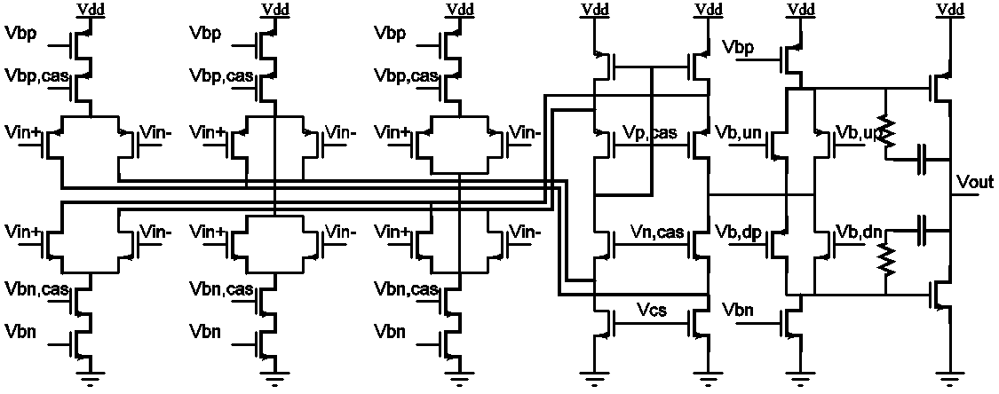
The first block utilizes a combination NFETs, which works at high input voltage, and PFETs, which works at low input voltage, to generate a constant transconductance against input common mode voltage. The second block sums up the signal from the first block, which is carried by four wires, into one signal runs on a single wire. The third block is a class AB power amplifier biased in subthreshold, so that the output voltage can reach the rails without too much gain loss in comparison to the gain in the middle of the rails.