
Introduction
This the project "RF Front-End Receiver for ISM-900M" webpage. It is the part of the course " VLSI Design Lab (E6350)",taught by Prof. Peter Kinget in Spring 2016 at Columbia University. Thanks MOSIS for kindly offering the opportunity to fabricate this chip
In this project, we designed a direct down conversion receiver front-end for ISM band. This wide-band receiver should also be able to operate in both the GSM-900MHz and GSM-1.8GHz band. The system-level block diagram of the chip is shown in Fig. 1. The receiver front-end is a homodyne receiver with direct down conversion. The chip consists of five modules: a low-noise amplifier (LNA), a I/Q clock generator, two mixers, two low-pass filters (LPF), and two variable gain amplifiers (VGA). The received signal by the antenna will be amplified by the LNA first, and then mixed with a clock signal to be downconverted to baseband. The clock I/Q generator will take an off-chip differential clock signal as an input and will generate two sets of differential clock signals with different phase shift to feed into the mixers. After the signal get down converted, the base band signal will be cleaned by a LPF, and the VGA will provide additional gains before the signal goes into the ADC.
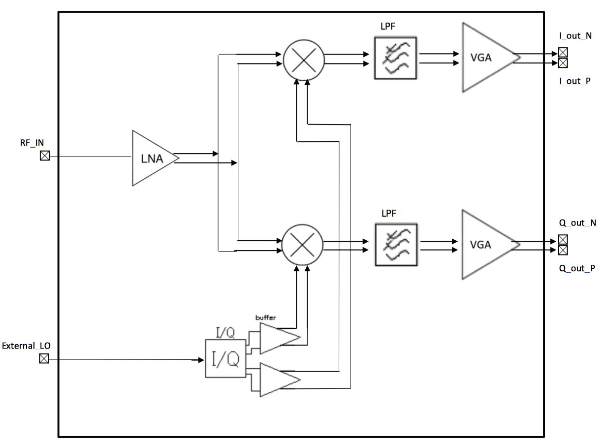
Figure 1 System Block Diagram
The photo of the die is emploeed in Fig.2. A QFN-28 package is used in this project in order to reduce the parasitics associated with the bond wires and packages.
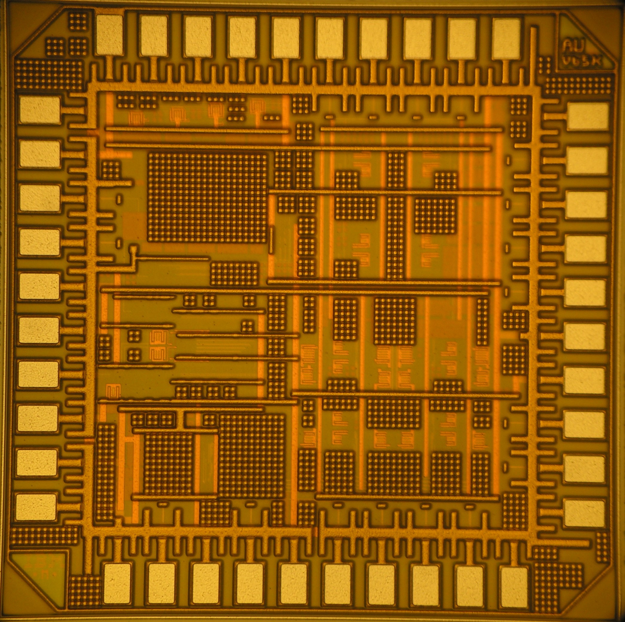
Figure 2 Die plot