References:
For further reading on pipelined A/D Converters, or to get a clear understanding, please refer to the following papers:- Lewis: JSSC Dec 1987
- Song: JSSC Dec 1988
- You can also refer to Johns and Martin, Analog Integrated Circuit Design, Chapter/Section 13.5, 13.8 for a very brief introduction on pipelined ADCs.
- For fundamentals on A/D conversion, definitions etc, refer to Johns and Martin, Analog Integrated Circuit Design, Chapter 11.
- A sample opamp design along with simulation techniques (Note, this is a single ended design. You need to develop a fully differential opamp.)
- You might want to refer to Middlebrook's loop gain simulation technique from the Links section of the course webpage.
Background:
A basic block diagram of a stage in a pipelined A/D converter is as below:
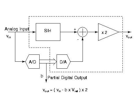
The entire circuit (and hence the opamp) has to be fully differential. It will be driving a switched capacitor circuit. Typically the contents of the dashed area in the diagram above might contain something as follows: (Note: This is just an example. The literature you will refer to might not contain a stage identical to this. There could be many different implementations of this block - each having its own advantages w.r.t sampling, charge injection, parasitics, offset etc. You do not have to use this circuit.)
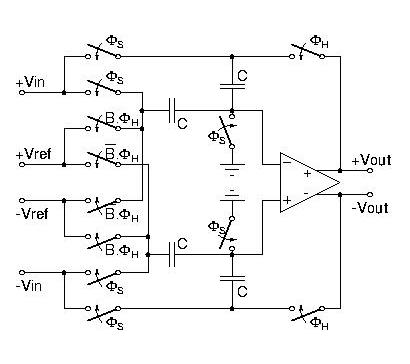
This circuit will be driving the next stage in the pipeline and so on. B and Bbar in the circuit are outputs of the A/D converter which is outside the dashed region. One might choose to use a 1 bit A/D (also known as a comparator) and a 1 bit D/A in one stage of the pipeline converter. There are more advanced architectures with 1.5 bit or even 2 bit stages, but we will not delve into these.
For your own understanding, you have to first analyze the block diagram (first picture) and see for yourself how a pipelined A/D works. You will realize that the accuracy of the complete A/D converter with all of its stages is completely defined by the accuracy of the dashed area of the first stage of the pipelined converter. Now, for you own understanding analyze the circuit (second picture) shown and see that indeed it does fit into the dashed area of the block diagram.
The goal of this project will be to design this dashed region of the block diagram. Given the accuracy required and the power budget for your circuit, design for the fastest sampling rate that you can achieve.
Design Procedure:
- System Level Design: (Time to allot: max 10 days, finish by
April 19)
- Choose size of the LSB. Determine capacitor size. Also, determine Vref.
- Choose the switch size.
- Determine the opamp specifications using the ideal opamp model given below (gain, bandwidth, stability, noise, distortion, settling, etc.)
- Use the opamp model and ideal switches and see if your design will work.
- Opamp Design: (Time to allot: max 15 days, finish by May 3)
- Design an opamp that satisfies these requirements; choose the topology; size transistors; verify specs.
- Design the switch.
- Make sure that the input referred noise is of the same order of magnitude as the noise of the switch.
- The opamp should have common mode feedback. Make sure that when you put the amplifier in a closed loop it does not start oscillating as a result of the common mode feedback. If it does, you need to compensate for common mode feedback.
- Overall Simulations: (Time to allot: max 8 days, finish by May 12)
- Plug in the opamp in the A/D stage and run through clock phases; prove the 2x amplification happens with the right accuracy; show that you have enough settling time, etc.
- Write the report.
Models:
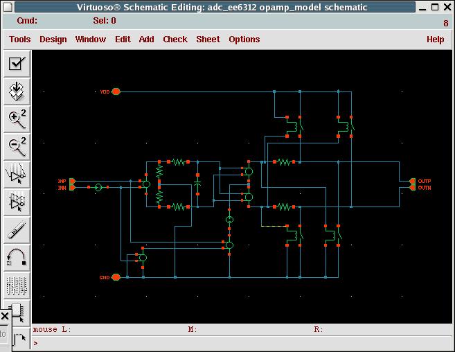
To figure out what specs you need for the opamp, a quick model has been implemented in cadence, which you can use. The model implements a two pole fully differential opamp, you can choose the common mode as well as differential mode gains, the output common mode, gain bandwidth, output resistance etc.Notes on the opamp model:
- This model is a two stage opamp model. The second pole is realized by Rout and the load capacitance you choose to use. If you want to make a single stage opamp, do not use this model as is. Copy it over and modify it to suit your needs.
- The model does not implement slew rate.
- The output common mode is implemented as:
output_common_mode = vcm + Acm * input_common_mode
(This means that if you have chosen vcm = 0.9V and your input_common_mode = 0.9V and Acm = 0.01, then output_common_mode will be 0.909V.) - The switches at the output node make sure that the voltages are limited within the power rails. No other non-linearity has been implemented.
Here is the schematic used for this:
You will need to add the following to your library path:
/home/user2/spring04/aj2112/ee6312models (call this ee6312models)
and the model is available in the cell called "opamp_model".
Please let me know if you
want more features added to the opamp model.
FAQ:
- Do we have to use the switched cap circuit that you have shown?
No, you don't have to. In fact, the circuit there has serious limitations w.r.t offset cancellation during sampling. Look up the papers and references and try to come up with your implementation of that block. You can use it if you really can't come up with anything else.
- How does the 3 mV offset on the comparator affect me? Does this mean
my LSB has to be 6 mV?
The 3 mV offset doesn't affect you much. For the pipelined stage, the DAC, S/H, adder, gain 2 block have to be n-1 bits accurate. The 1 bit comparator doesn't need to be as accurate. The accuracy of the comparator will hit you as INL/DNL - but for now, you need not worry about it. As long as the rest of your circuitry (DAC, S/H etc) are accurate, you pass on a correct analog output to the following pipeline stage.
- Can I assume linear capacitors?
Yes.
- Do I have to generate the clocks?
No. Assume that these have been given.
- Do I have to generate Vref?
No. Assume that this voltage has been given.