HW 4
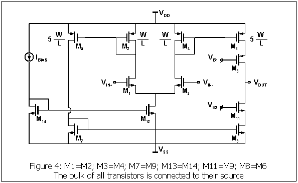
Figure 4 shows an operational amplifier with
differential input and single ended output. The relevant sizes of some
transistors are shown. Further assume VDD=5, VSS=0, and
assume that all transistors are sized so that VTn=-VTp=0.8V and (VGS - VT)n =-(VGS - VT)p=0.2V.
You can also assume that M1, M2, M3, M4, M5, M7, M13 and M14 have a lambda=0.
A. Calculate the maximum value of VB1 so
that all transistors are in the active region.
|
Expression: |
VB1-max = |
|
Value: |
VB1-max = |
B. Derive the minimum value of VB2 so that
all transistors are in the active region.
|
Expression: |
VB2-min = |
|
Value: |
VB2-min = |
For all the following questions, assume the values of VB1
and VB2 that you calculated in A & B.
C. Derive symbolically the gain of the amplifier for a
differential input signal i.e. VOUT/VIN
|
Expression: |
VOUT/VIN
= |
D. Derive common mode input range so that all
transistors remain in the active region. Indicate for each limit which
transistor(s) go(es) out of
active region first.
|
Transistor(s) |
|
-------------------------- |
|
|
Expression: |
<= VIncommon-mode <= |
||
|
Values: |
<= VIncommon-mode <= |
||
E. Derive output range so that all transistors remain
in the active region. Indicate for each limit which transistor(s) go(es) out of active region first.
|
Transistor(s) |
|
-------------------------- |
|
|
Expression: |
<= VOUT
<= |
||
|
Values: |
<= VOUT
<= |
||
F. Now assume that the devices have a non-zero output
conductance (i.e. lambda is not zero). Find an expression for the common mode
gain. You can make approximations if necessary. Explain your reasoning and
justify your assumptions.
G. Find a expression for the CMRR i.e. (differential
mode gain)/(common mode gain).