EE6312: Homework Assignment 3
-
Sketch Vout vs Vin for the following circuits as Vin varies from 0 to Vdd. Identify important transition points.
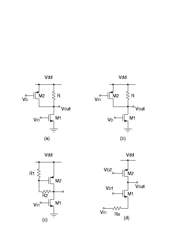
(Problem number 3.16 from Design of Analog CMOS Integrated Circuits, Behzad Razavi)
-
Small Design Problem:
(a) Using 1.8V devices and a 1.8V supply, design a common source amplifier with a resistive load. Design for maximum gain. Keep the device in strong inversion
and design for an output swing of 1.5V. Out of the device matrix we used before
(WxL, Wx3L, Wx9L, 3WxL 3Wx3L etc) pick a device size so that you get minimum power consumption.Document your results with DC and AC simulations.
(b) Repeat (a) for 3.3V devices and 3.3V power supply and 3V
output swing.
Submission:
For the first problem, you are welcome to do simulations, but analytical
expressions for the important transition points are required. For these, you
can use a plain text or any fancy formatting that you would like to. For the
second problem please hand in schematics, simulation plots and a brief explanation of how
you designed this. Once again, please compile everything in one big pdf file and
send it.
Due Date:
March 3, 2004